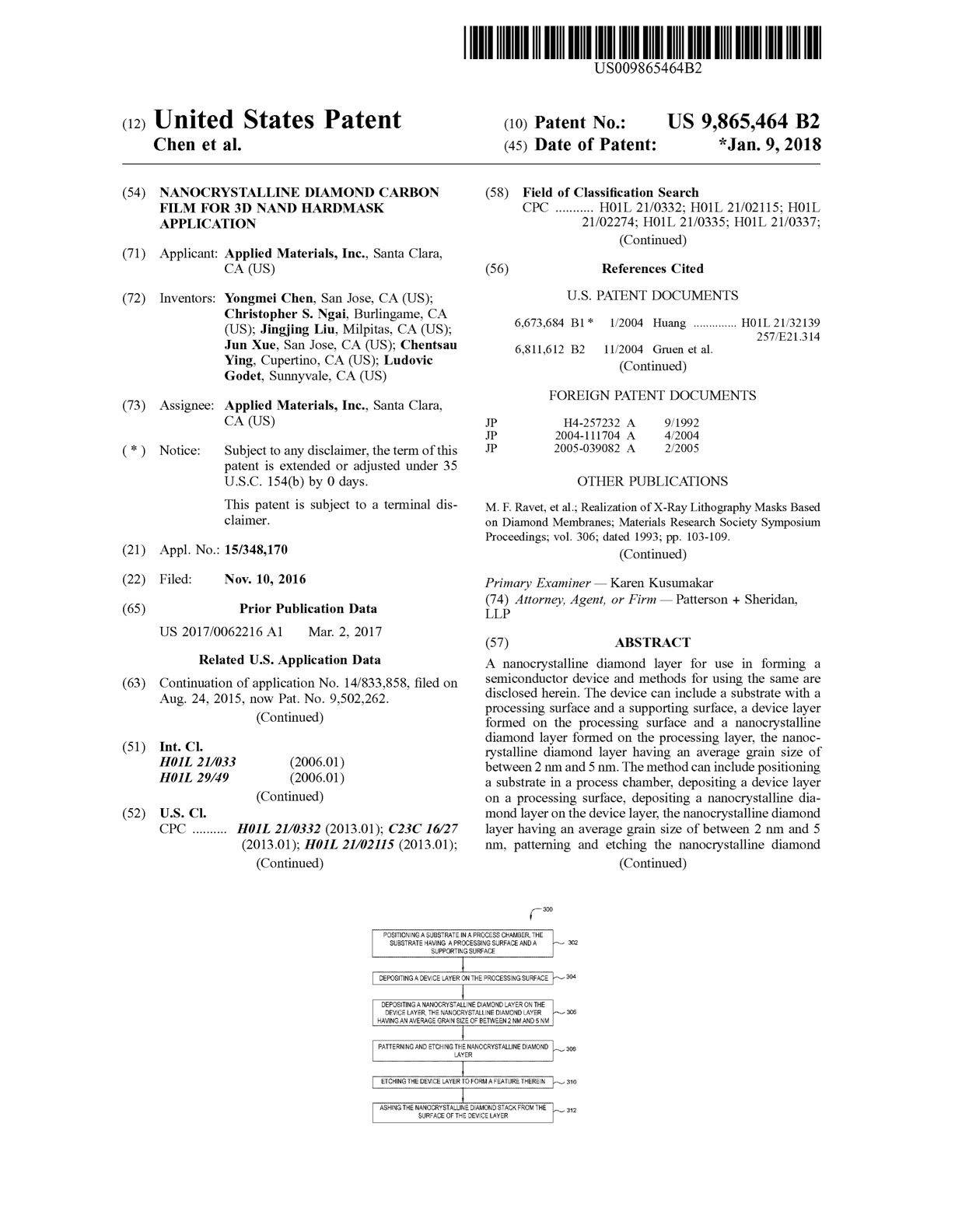
Ludovic Godet2022-01-07T01:04:40-05:00 US 9,865,464: Nanocrystalline diamond carbon film for 3D NAND hardmask application
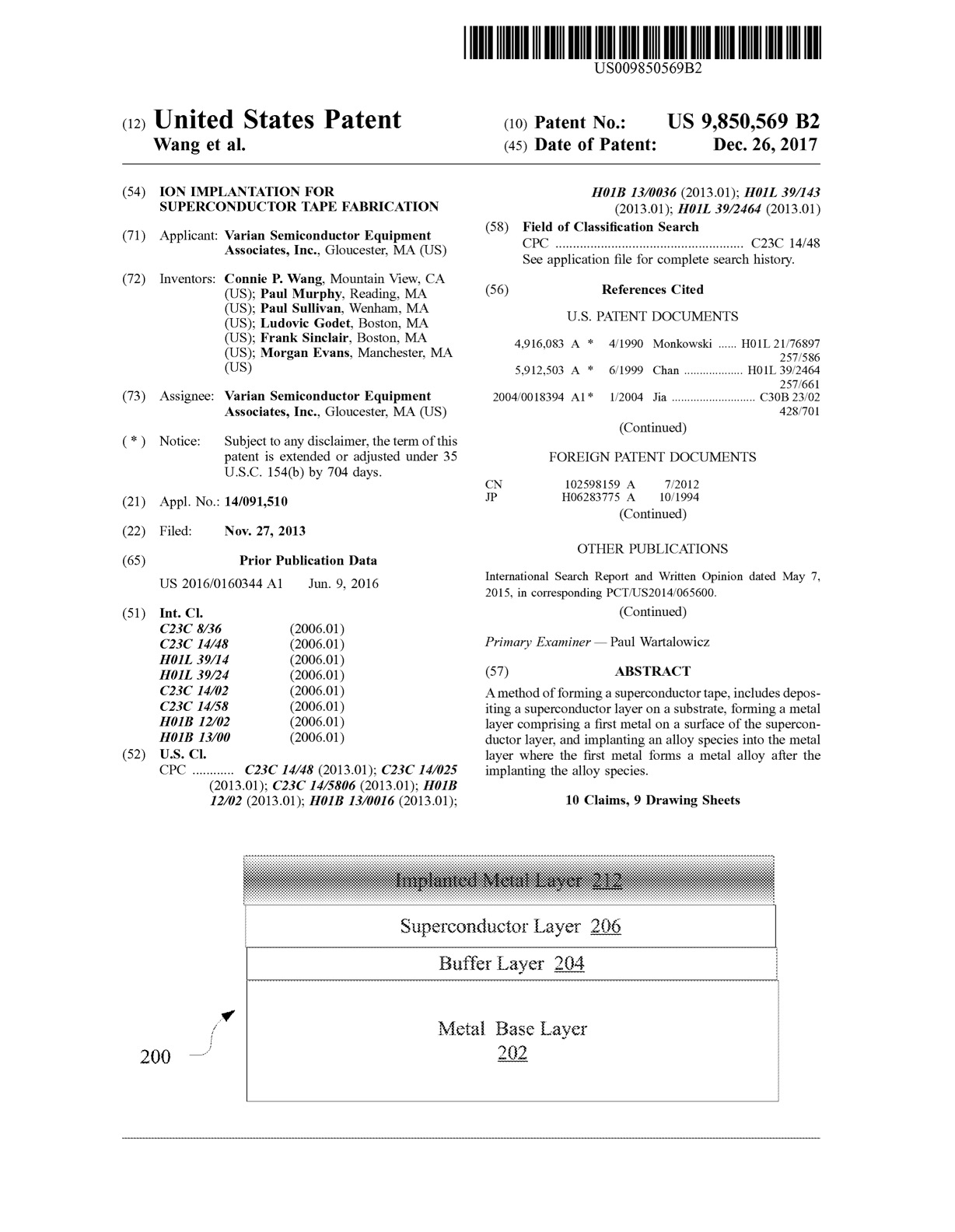
Ludovic Godet2022-01-07T00:47:58-05:00 US 9,850,569: Ion implantation for superconductor tape fabrication
Staff2021-01-31T18:33:30-05:00 US 9,515,166: Selective Atomic Layer Deposition Process Utilizing Patterned Self-Assembled Monolayers for 3D Structure Semiconductor Applications
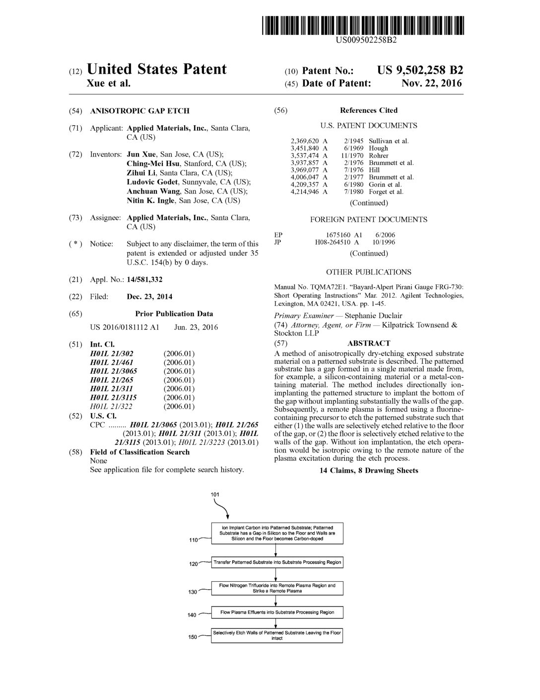
Staff2021-01-31T19:25:57-05:00 US 9,512,517: Multiple Exposure Treatment for Processing a Patterning Feature
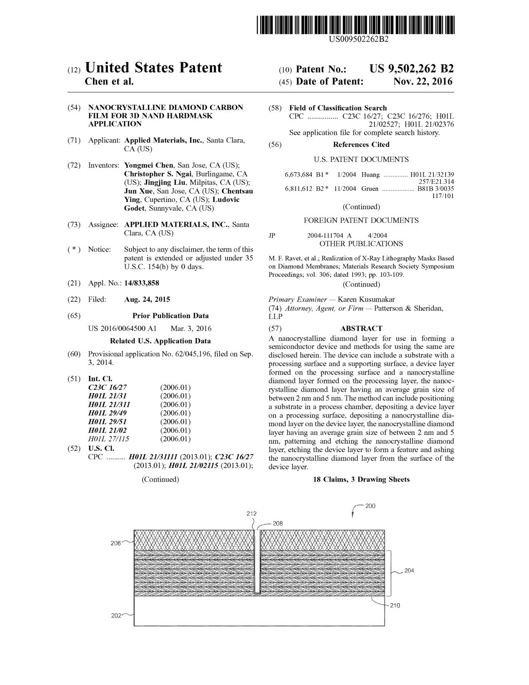
Staff2021-01-31T19:24:49-05:00 US 9,502,262: Nanocrystalline Diamond Carbon Film for 3D NAND Hardmask Application
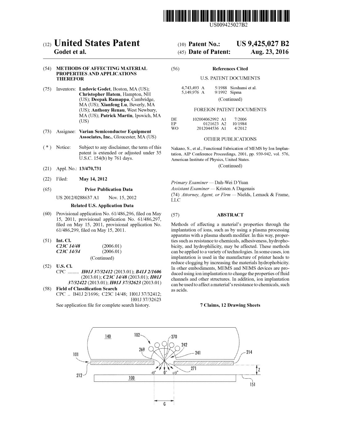
Staff2021-01-31T19:18:41-05:00 US 9,425,027: Methods of Affecting Material Properties and Applications
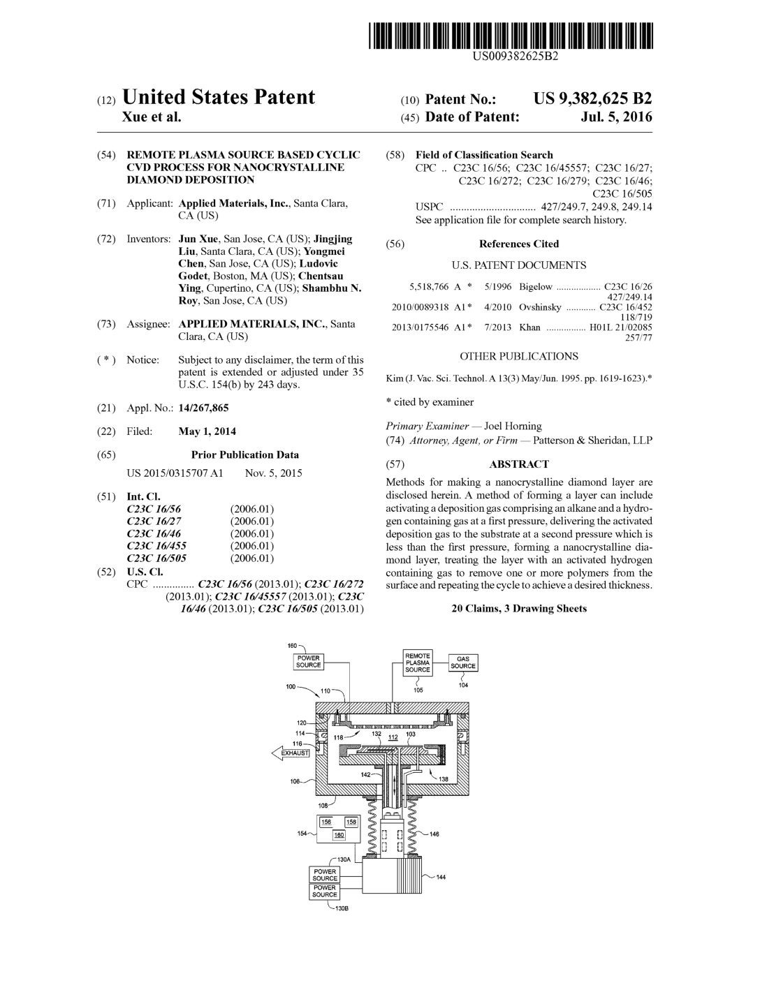
Staff2021-01-31T19:10:44-05:00 US 9,382,625: Remote Plasma Source Based Cyclic CVD Process for Nanocrystalline Diamond Deposition
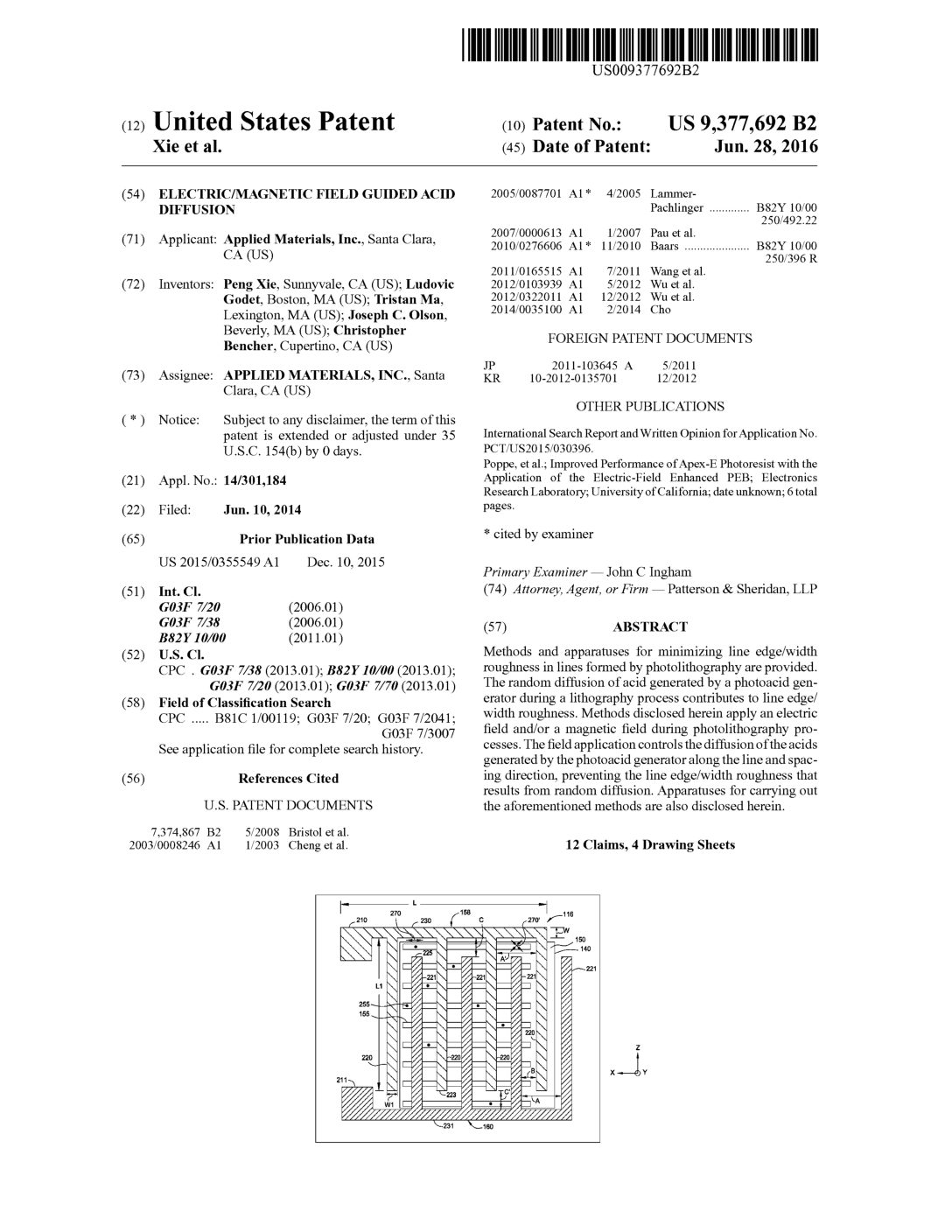
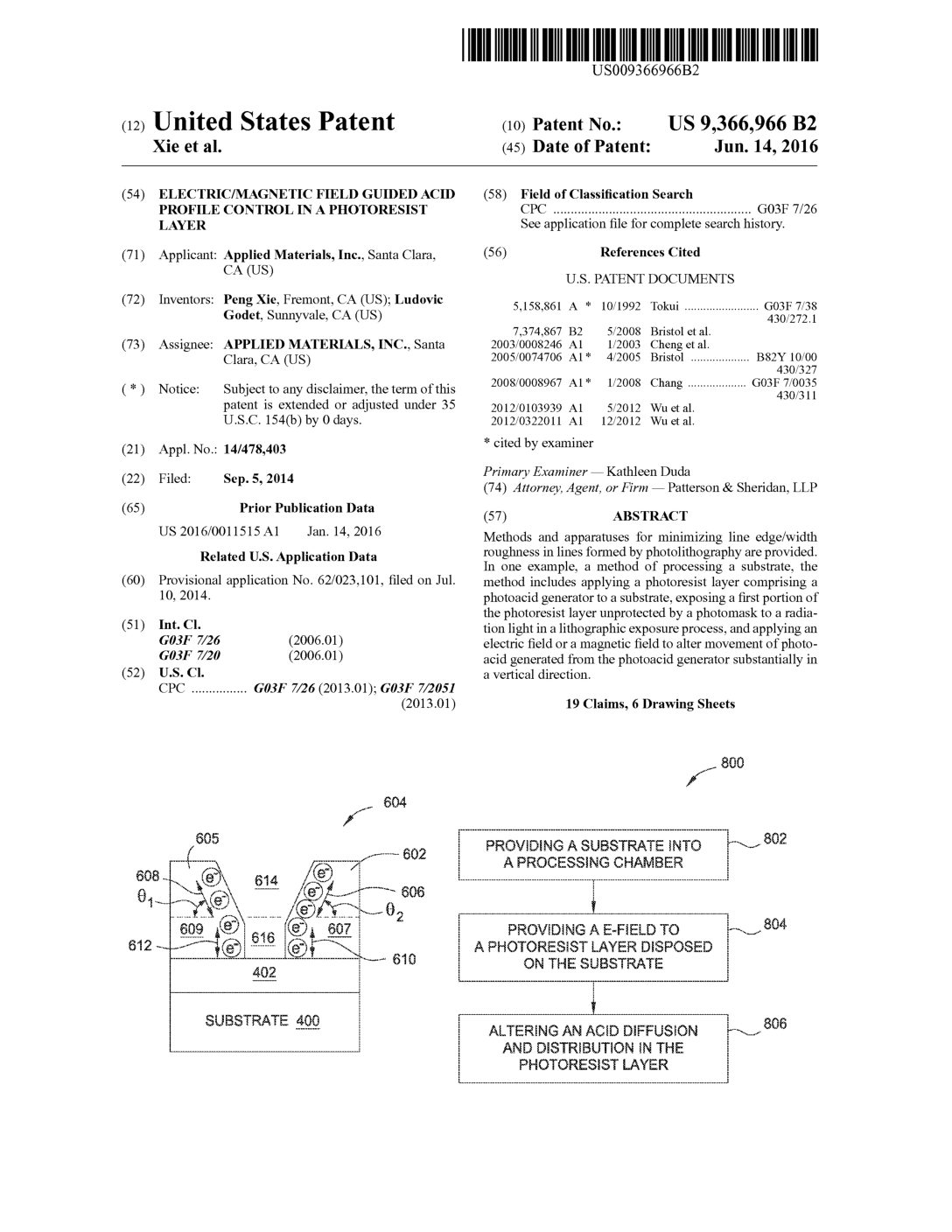
Staff2021-01-31T19:06:53-05:00 US 9,366,966: Electric/magnetic Field Guided Acid Profile Control in a Photoresist Layer
Staff2021-01-31T18:54:16-05:00 US 9,214,377: Methods for Silicon Recess Structure in a Substrate by Utilizing a Doping Layer
Staff2021-01-31T18:52:41-05:00 US 9,190,498: Technique for Forming a FinFET Device using Selective Ion Implantation
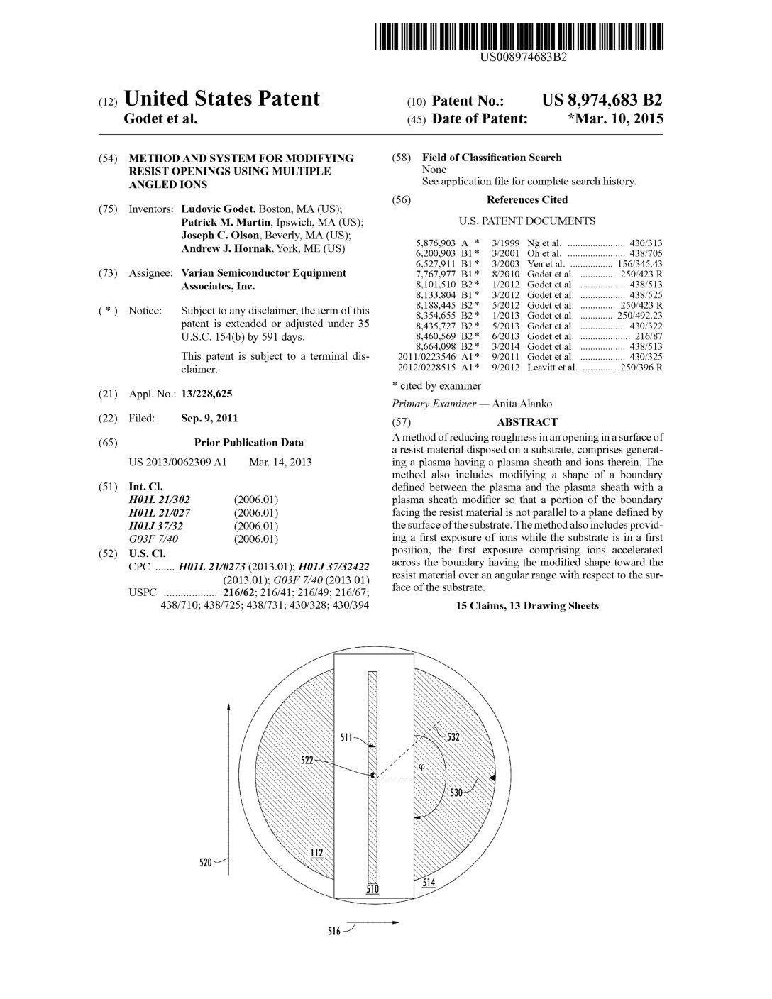
Staff2021-02-01T11:33:50-05:00 US 8,974,683: Method and System for Modifying Resist Openings using Multiple Angled Ions
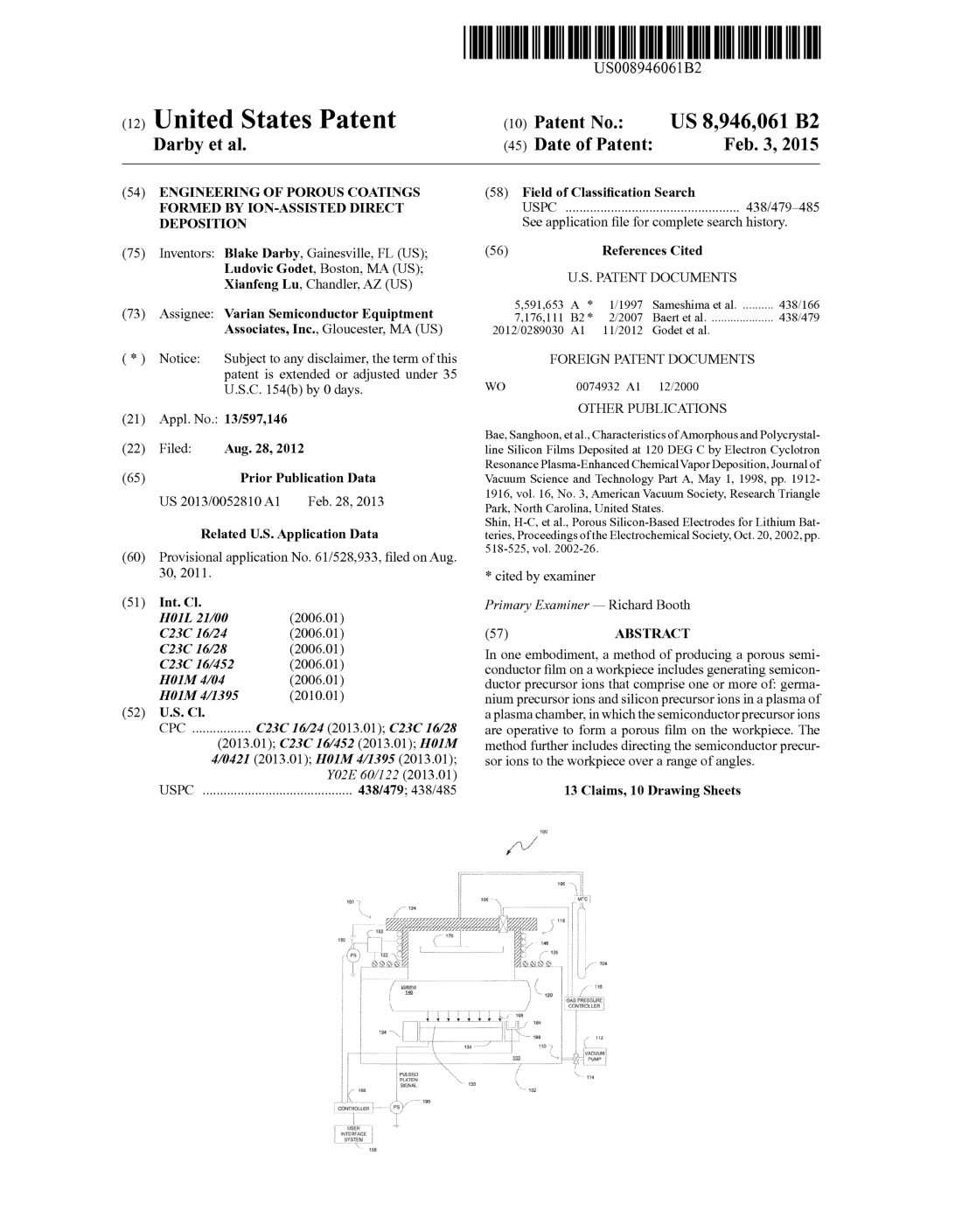
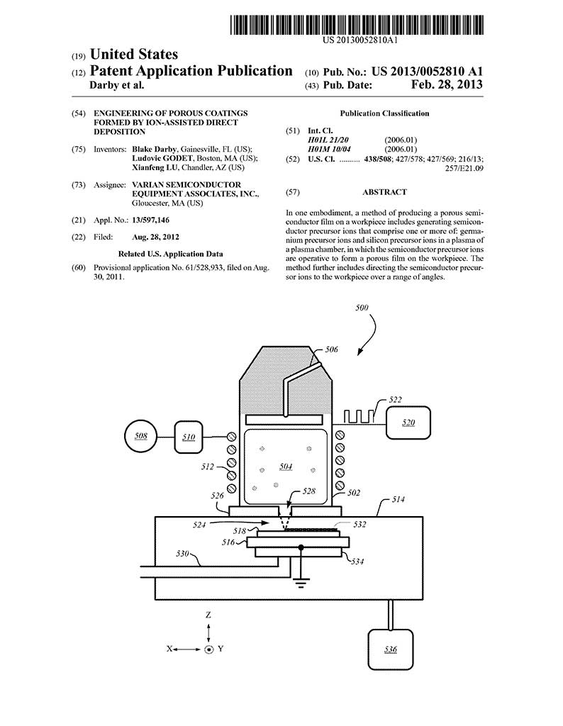
Staff2021-02-01T12:25:48-05:00 US 8,946,061: Engineering of Porous Coatings Formed by Ion-assisted Direct Deposition
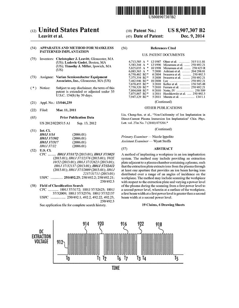
Staff2021-02-03T11:39:05-05:00 US 8,907,307: Apparatus and Method for Maskless Patterned Implantation
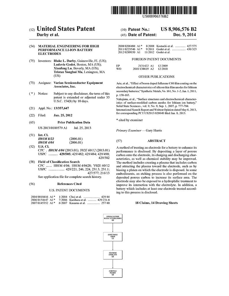
Staff2021-02-03T11:59:40-05:00 US 8,906,576: Material Engineering for High Performance Li-ion Battery Electrodes
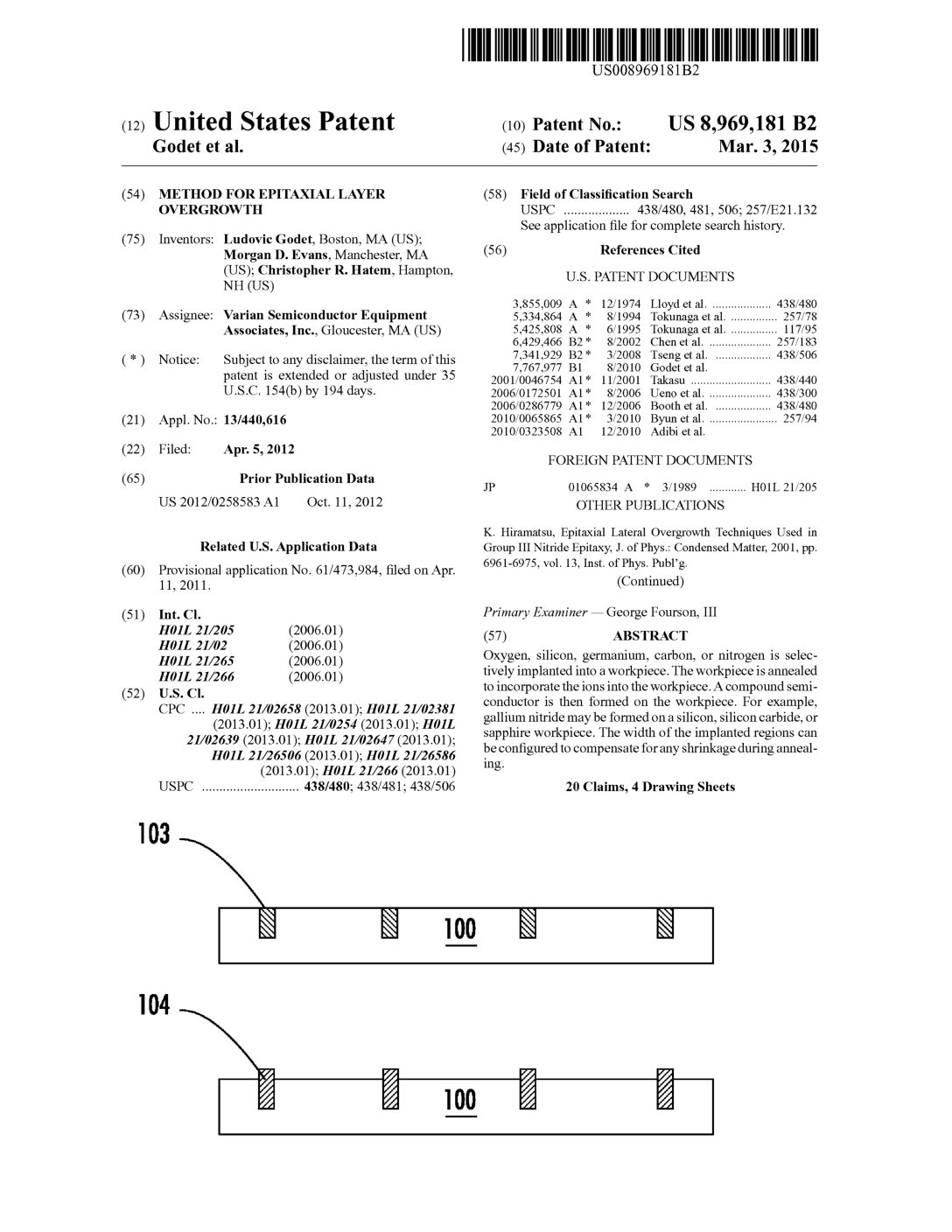
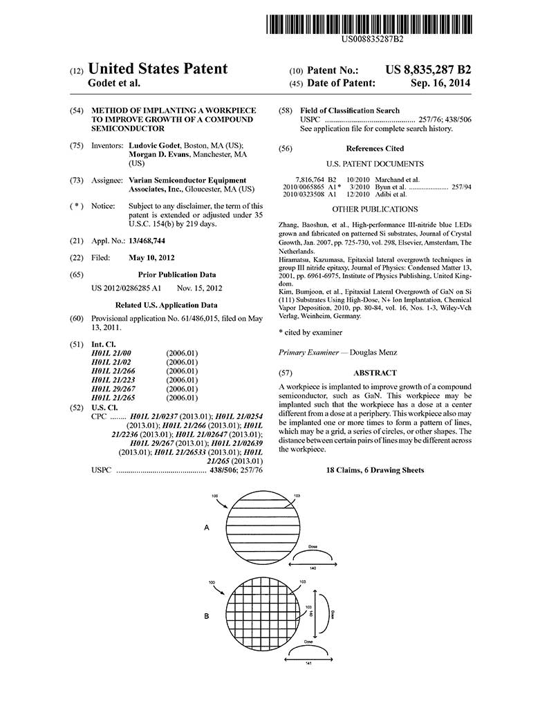
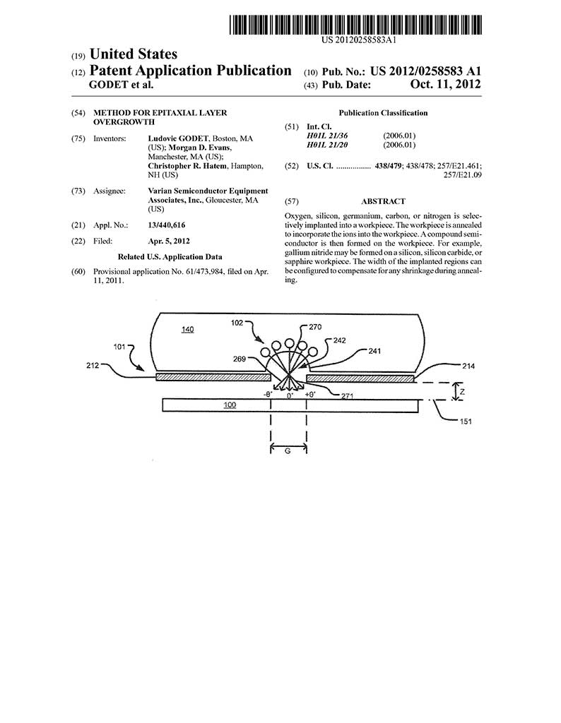
Staff2021-02-03T11:49:45-05:00 US 8,835,287: Method of Implanting a Workpiece to Improve Growth of a Compound Semiconductor
Staff2021-02-02T15:41:12-05:00 US 8,697,549: Deposition of Porous Films for Thermoelectric Applications
Staff2021-02-03T11:27:38-05:00 US 8,461,030: Apparatus and method for controllably implanting workpieces
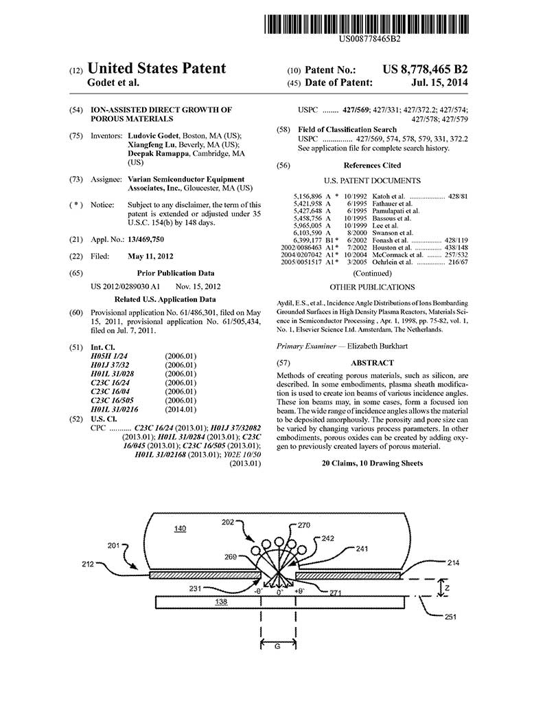
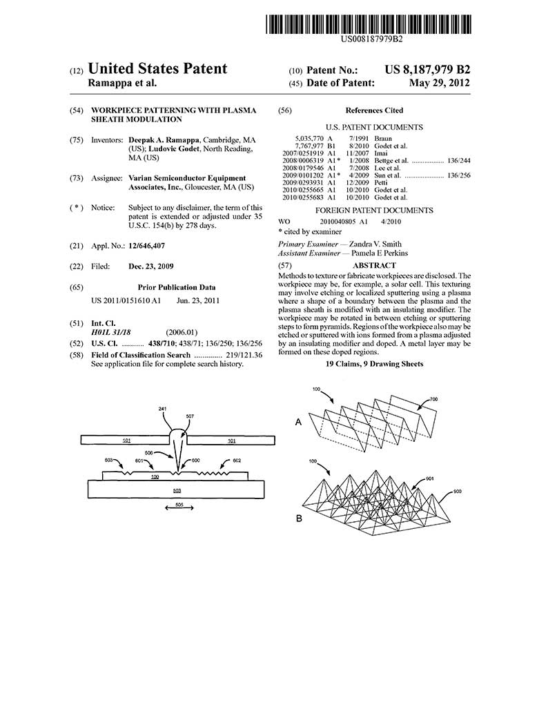
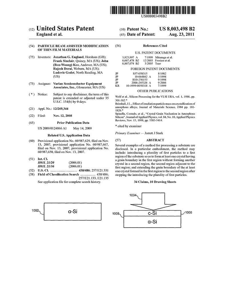
Staff2021-02-02T15:37:21-05:00 US 8,003,498: Particle Beam Assisted Modification of Thin Film Materials
Staff2021-02-02T09:57:01-05:00 US 20130052810: Engineering of Porous Coatings Formed by Ion–Assisted Direct Deposition
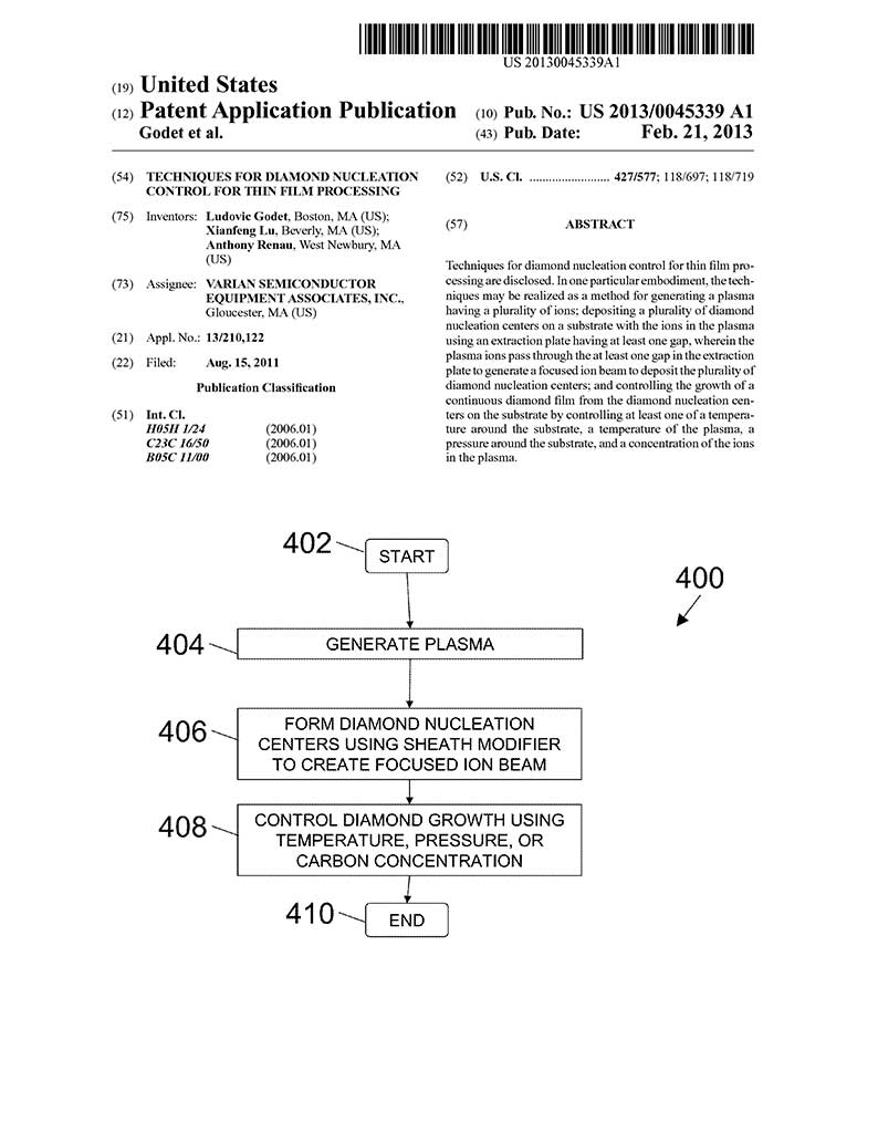
Staff2021-02-01T13:25:37-05:00 US 20130045339: Techniques for Diamond Nucleation Control for Thin Film Processing
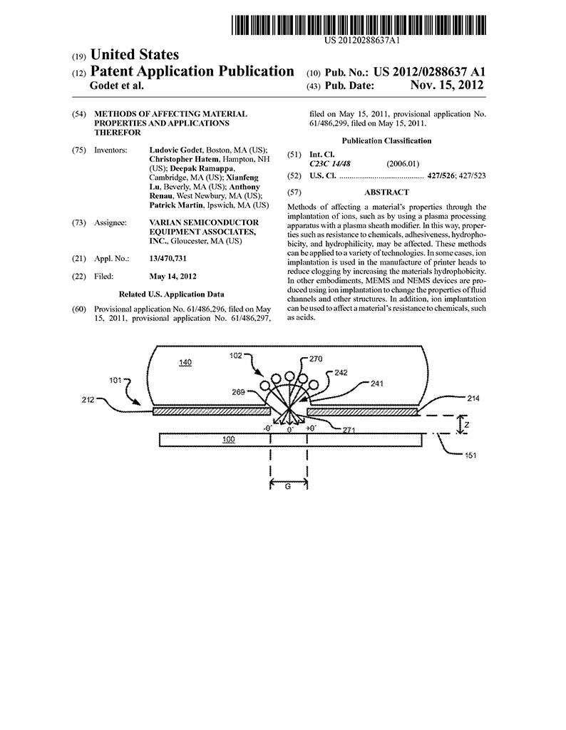
Staff2021-02-01T13:21:04-05:00 US 20120288637: Method of Affecting Material Proprieties and Applications
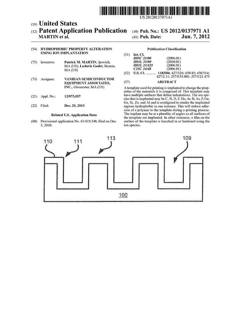
Staff2021-02-01T13:12:39-05:00 US 20120137971: Hydrophobic Propriety Alteration using Ion Implantation
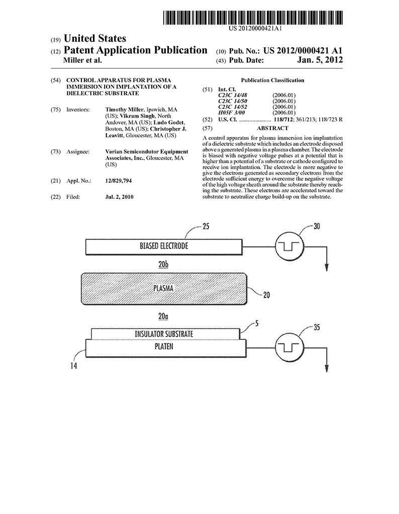
Staff2021-02-02T09:51:43-05:00 US 20120000421: Control Apparatus for Plasma Immersion Ion Implantation of Dielectric Substrate
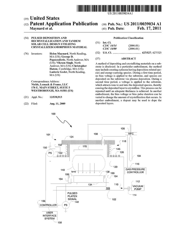
Staff2021-02-02T09:51:03-05:00 US 20110039034: Pulsed deposition and recrystallization and tandem solar cell design utilizing crystallized/amorphous material
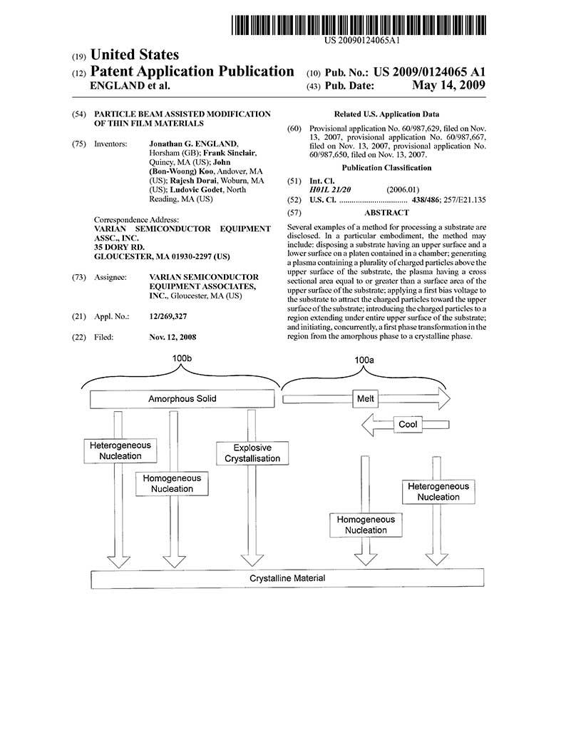
Staff2021-02-01T13:03:27-05:00 US 20090124065: Particle Beam Assisted Modification Of Thin Film Materials
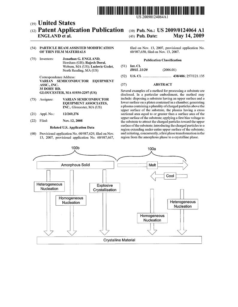
Staff2021-02-01T12:56:54-05:00 US 20090124064: Particle Beam Assisted Modification Of Thin Film Materials
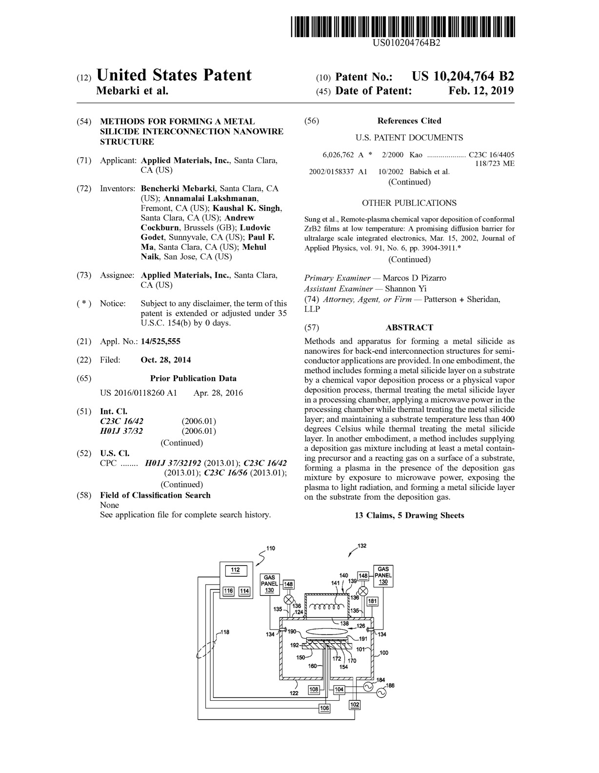
Ludovic Godet2022-01-10T14:16:23-05:00 US 10,204,764: Methods for forming a metal silicide interconnection nanowire structure
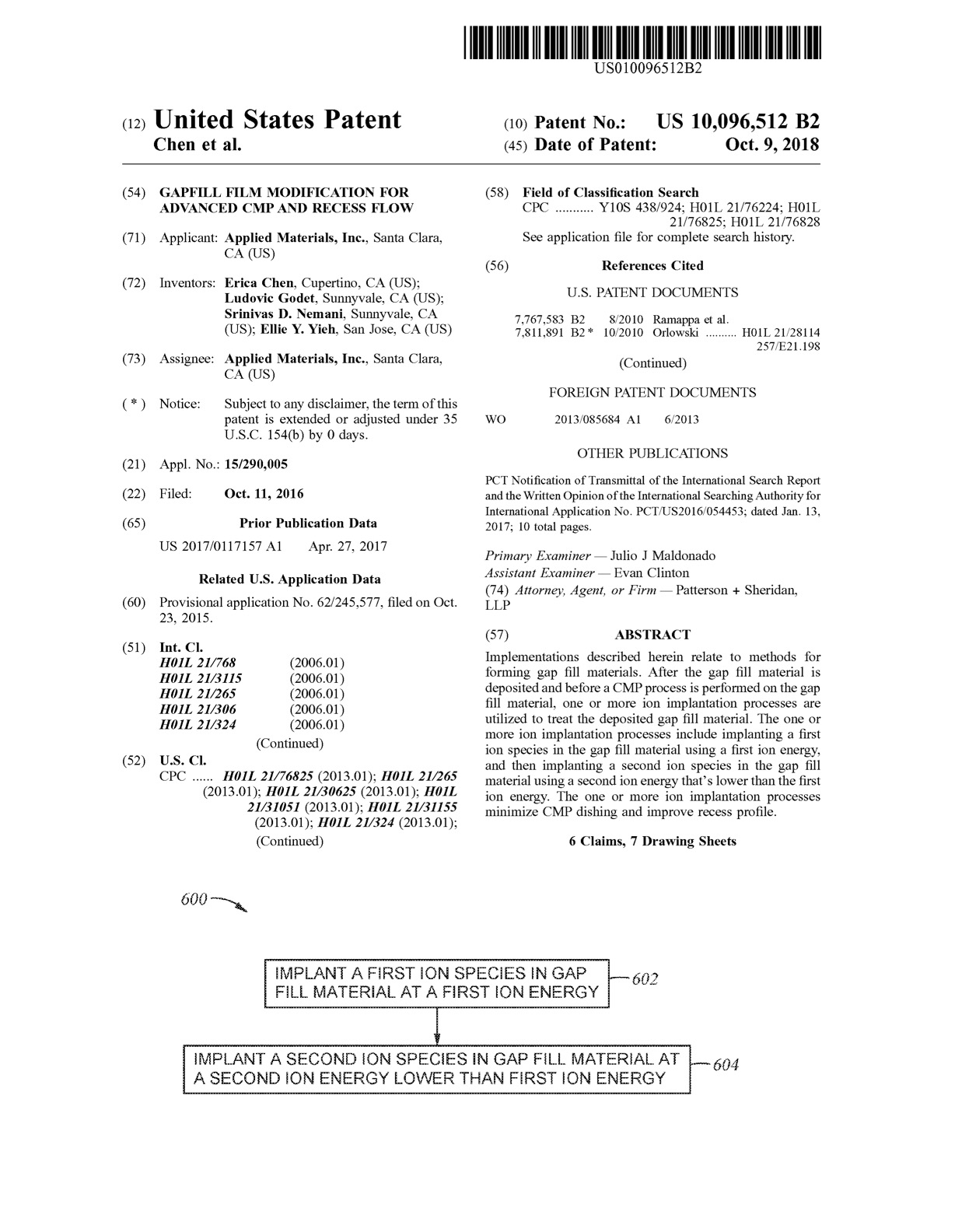
Ludovic Godet2022-01-07T01:48:01-05:00 US 10,096,512: Gapfill film modification for advanced CMP and recess flow


Social Media