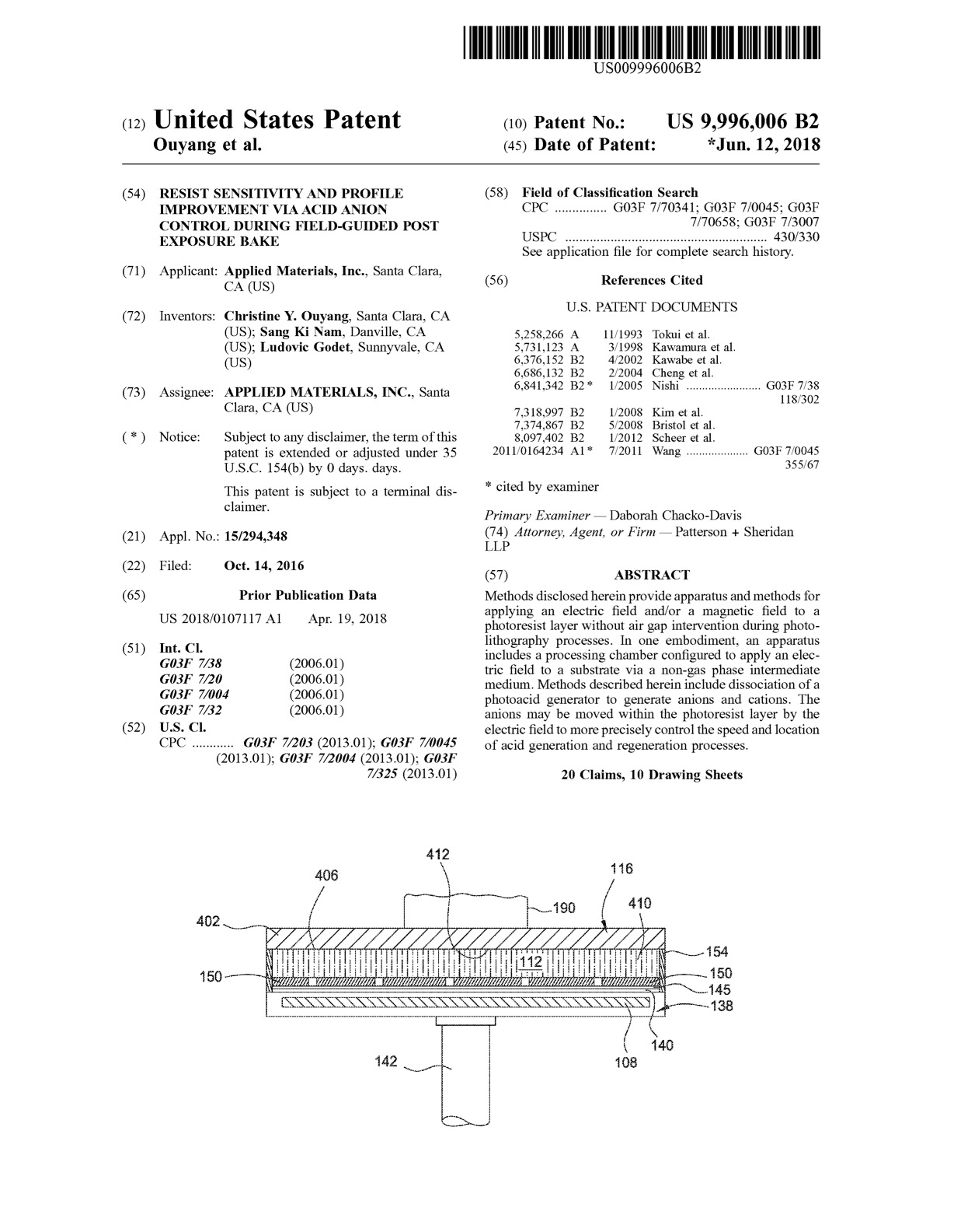
Ludovic Godet2022-01-07T01:34:06-05:00 US 9,996,006: Resist sensitivity and profile improvement via acid anion control during FGPEB
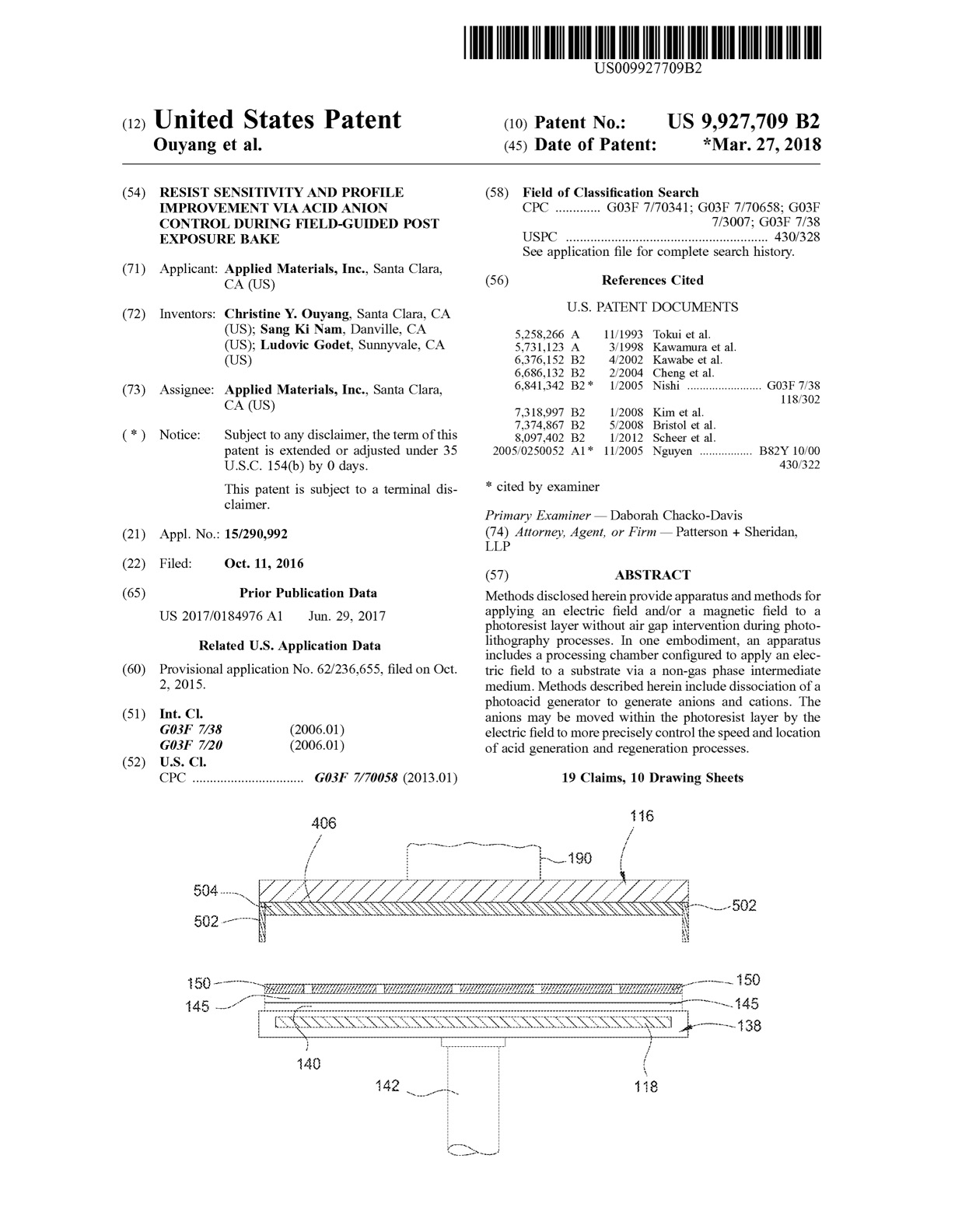
Ludovic Godet2022-01-07T01:21:29-05:00 US 9,927,709: Resist sensitivity and profile improvement via acid anion control during FGPEB
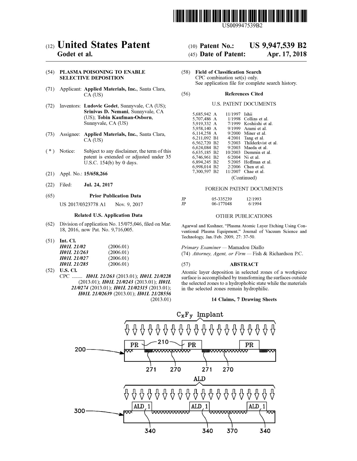
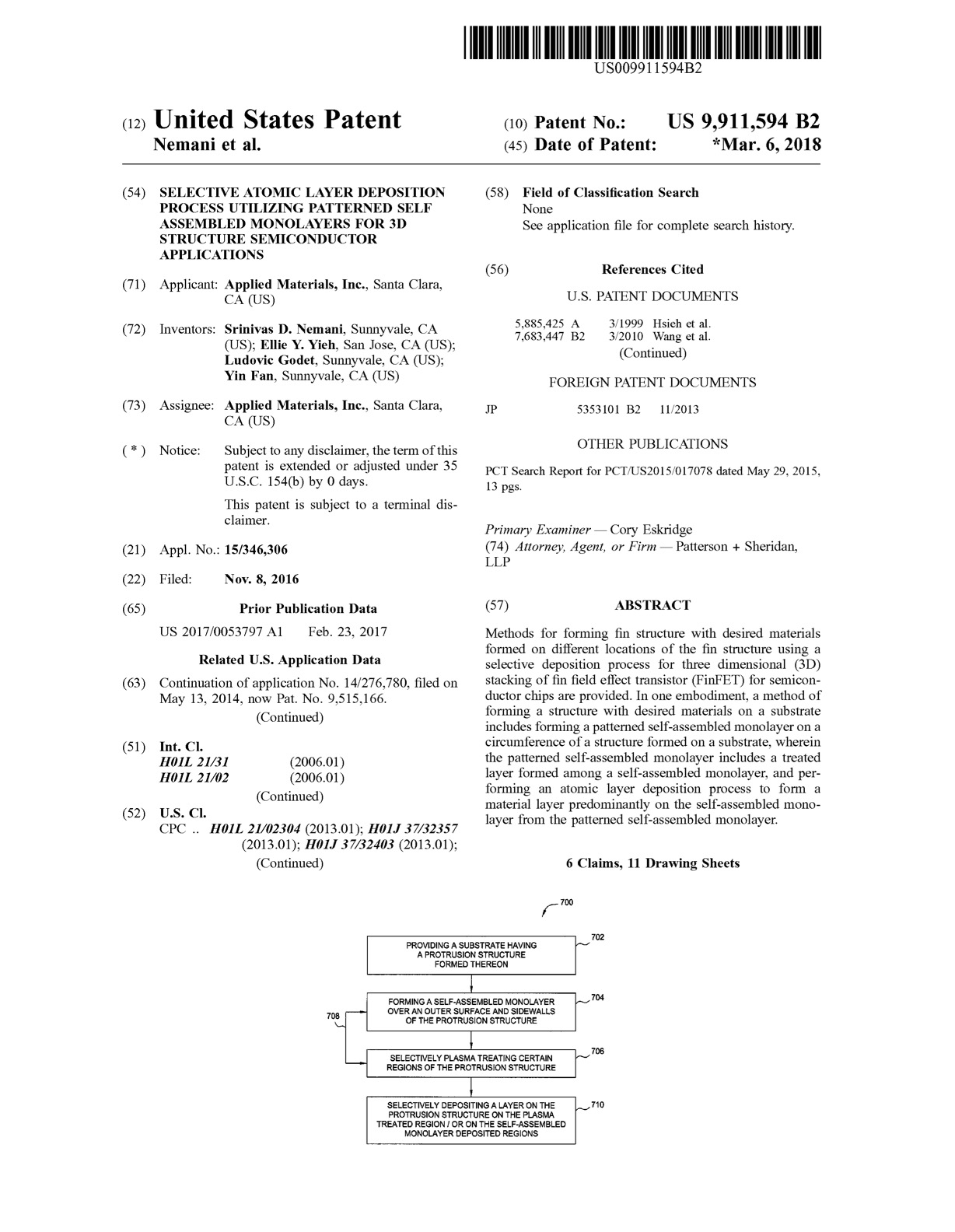
Ludovic Godet2022-01-07T01:18:47-05:00 US 9,911,594: Selective atomic layer deposition process utilizing patterned SAM for 3D structure application
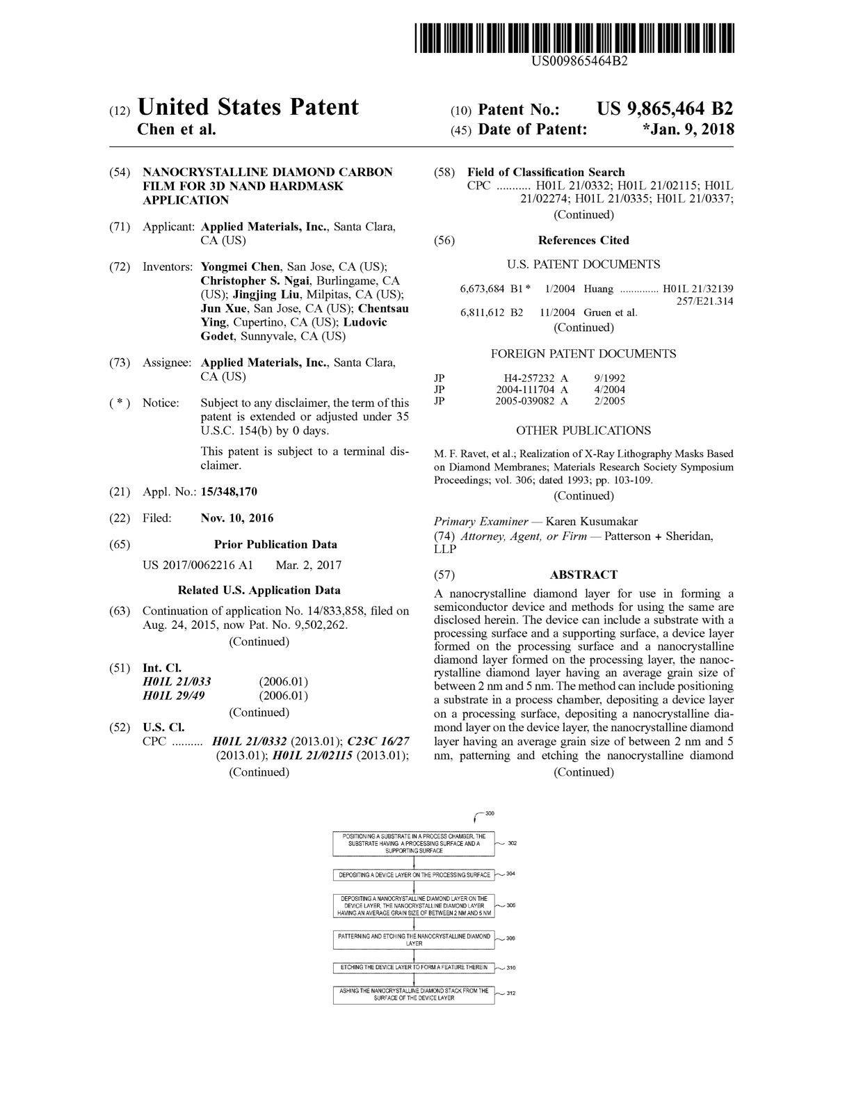
Ludovic Godet2022-01-07T01:04:40-05:00 US 9,865,464: Nanocrystalline diamond carbon film for 3D NAND hardmask application
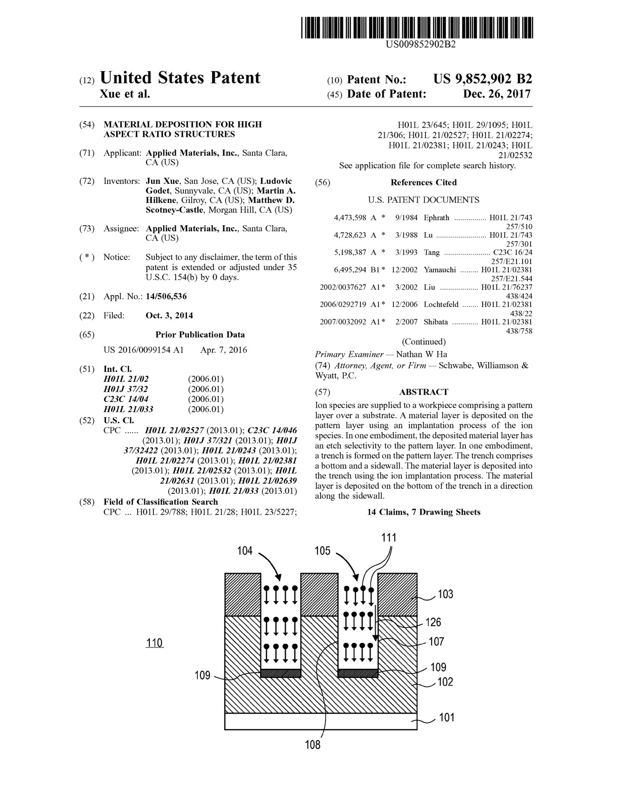
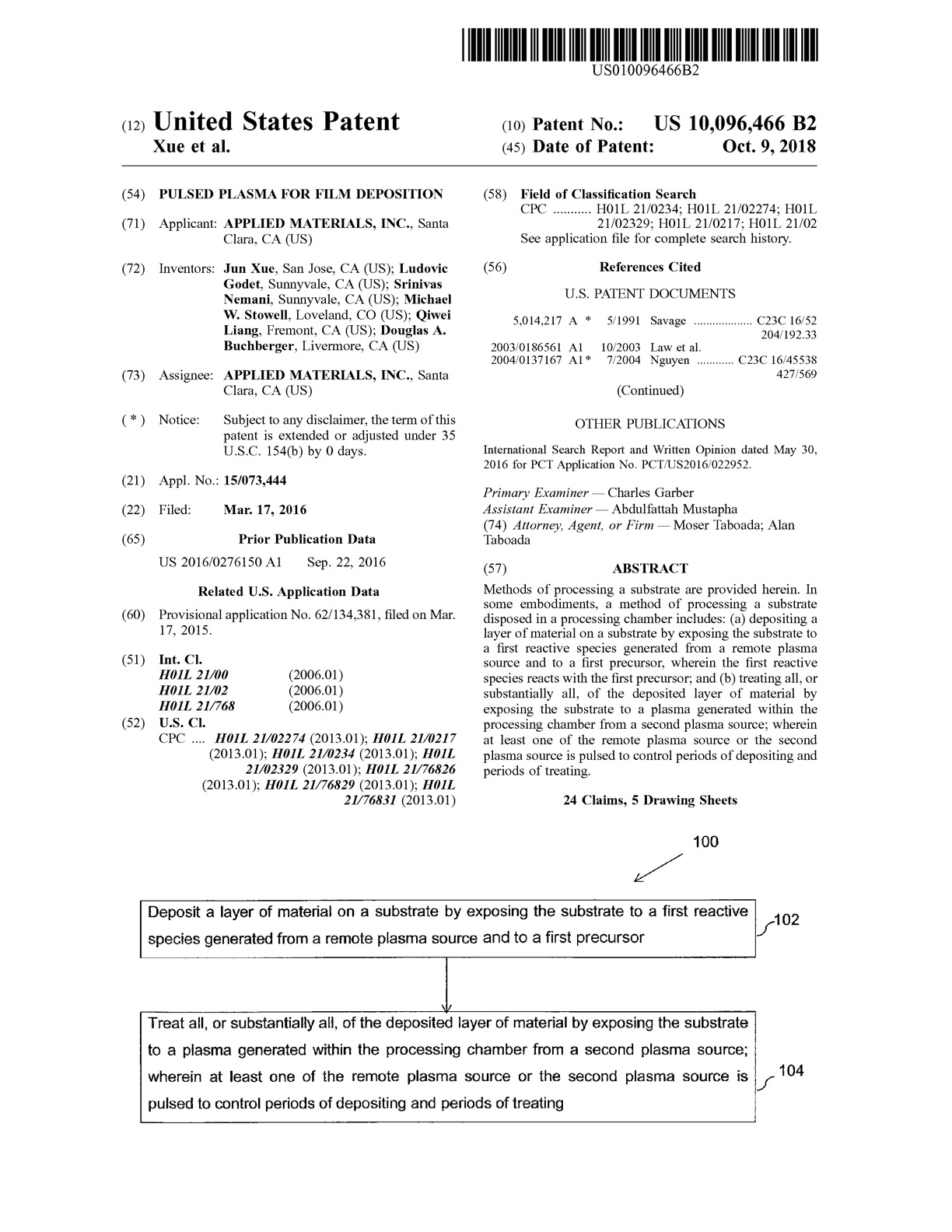
Ludovic Godet2022-01-07T00:55:46-05:00 US 9,852,902: Material deposition for high aspect ratio structures
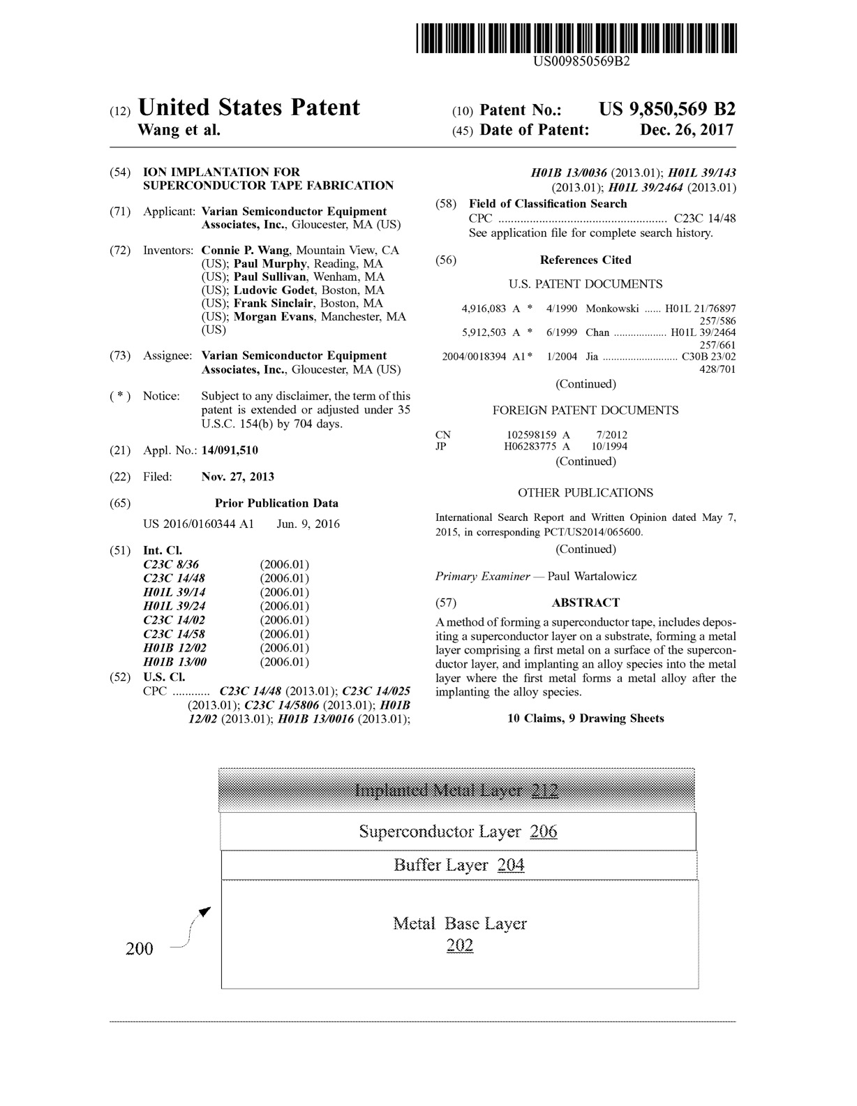
Ludovic Godet2022-01-07T00:47:58-05:00 US 9,850,569: Ion implantation for superconductor tape fabrication
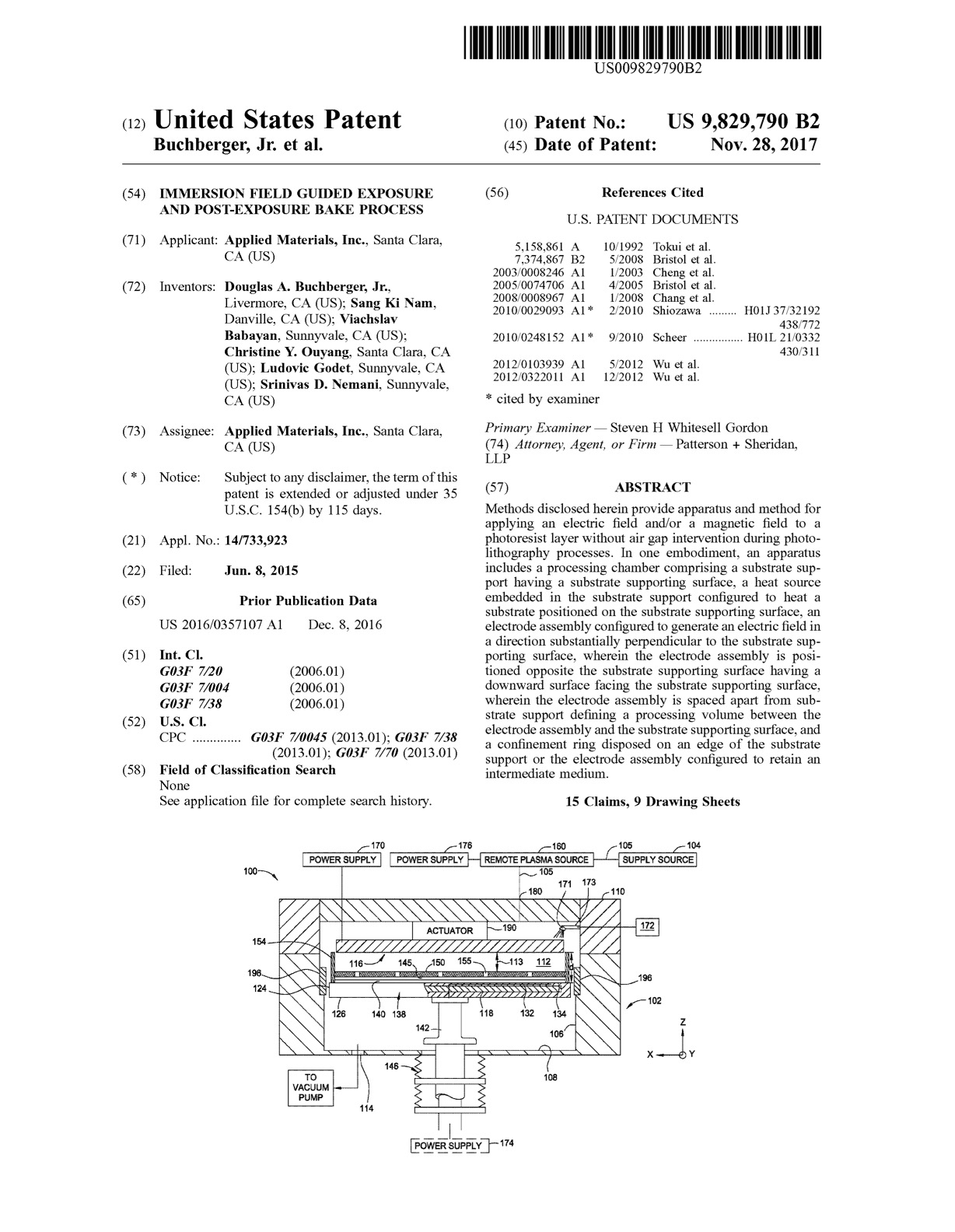
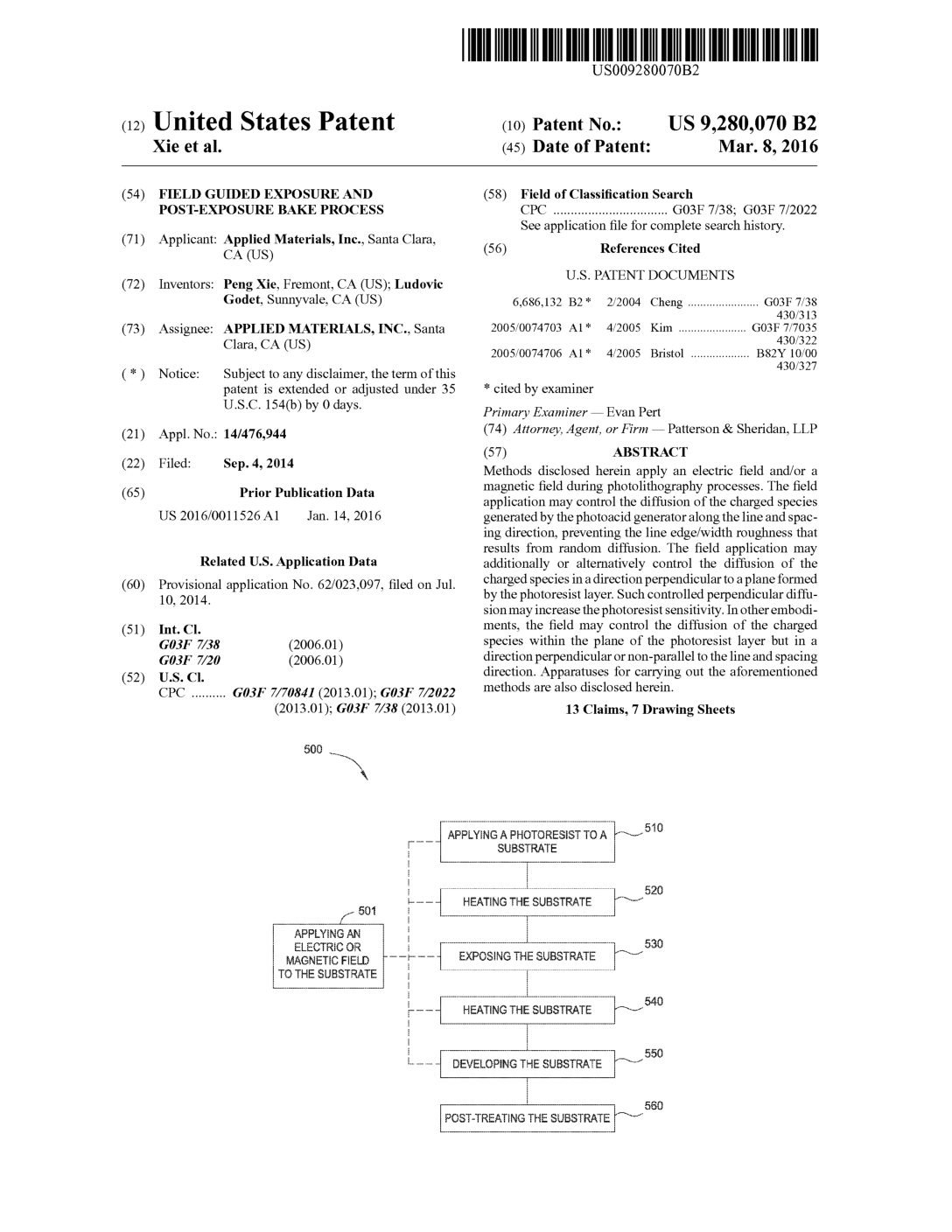
Ludovic Godet2022-01-07T00:40:39-05:00 US 9,829,790: Immersion field guided exposure and post-exposure bake process
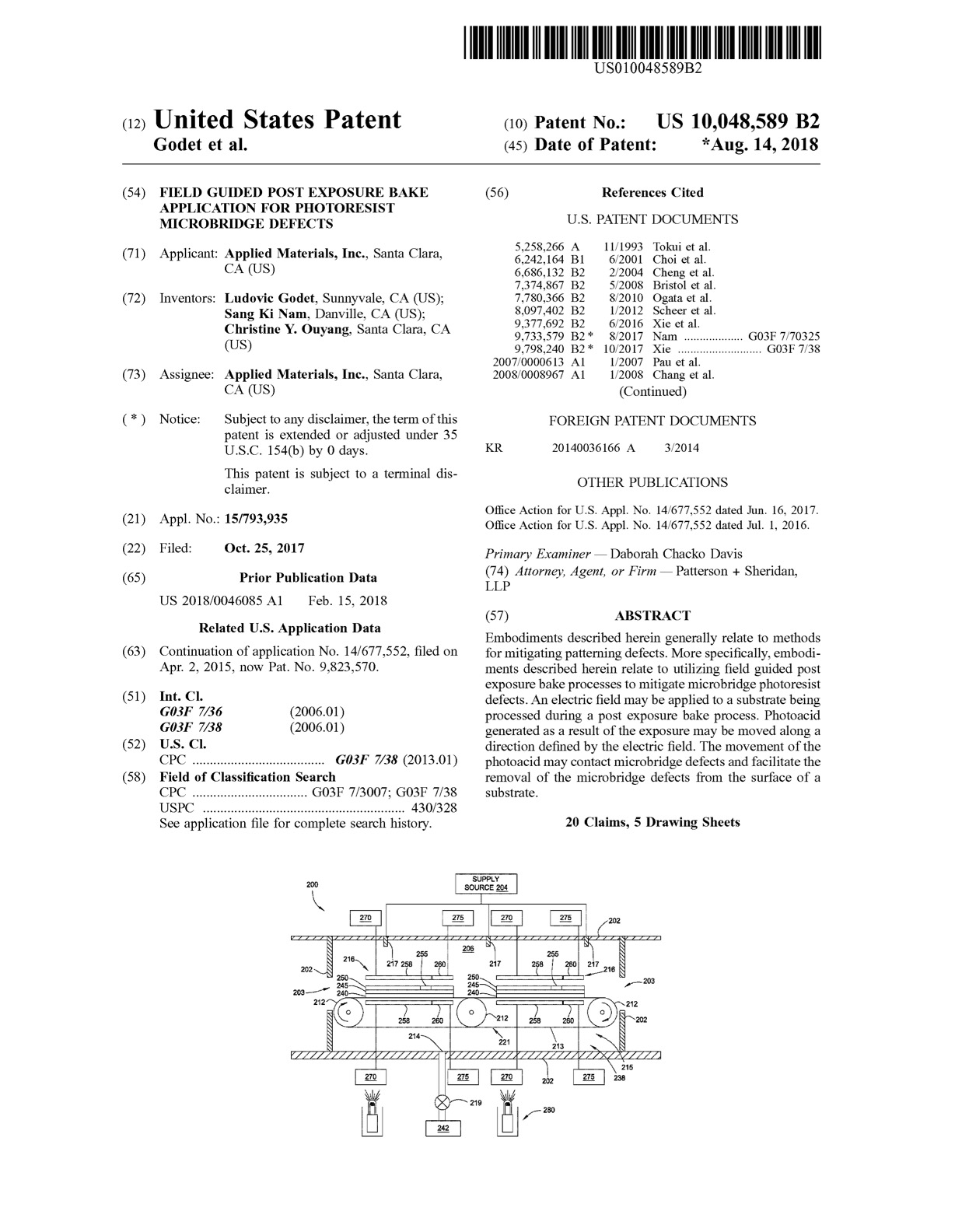
Ludovic Godet2022-01-07T00:37:07-05:00 US 9,823,570: Field guided post exposure bake application for photoresist microbridge defects
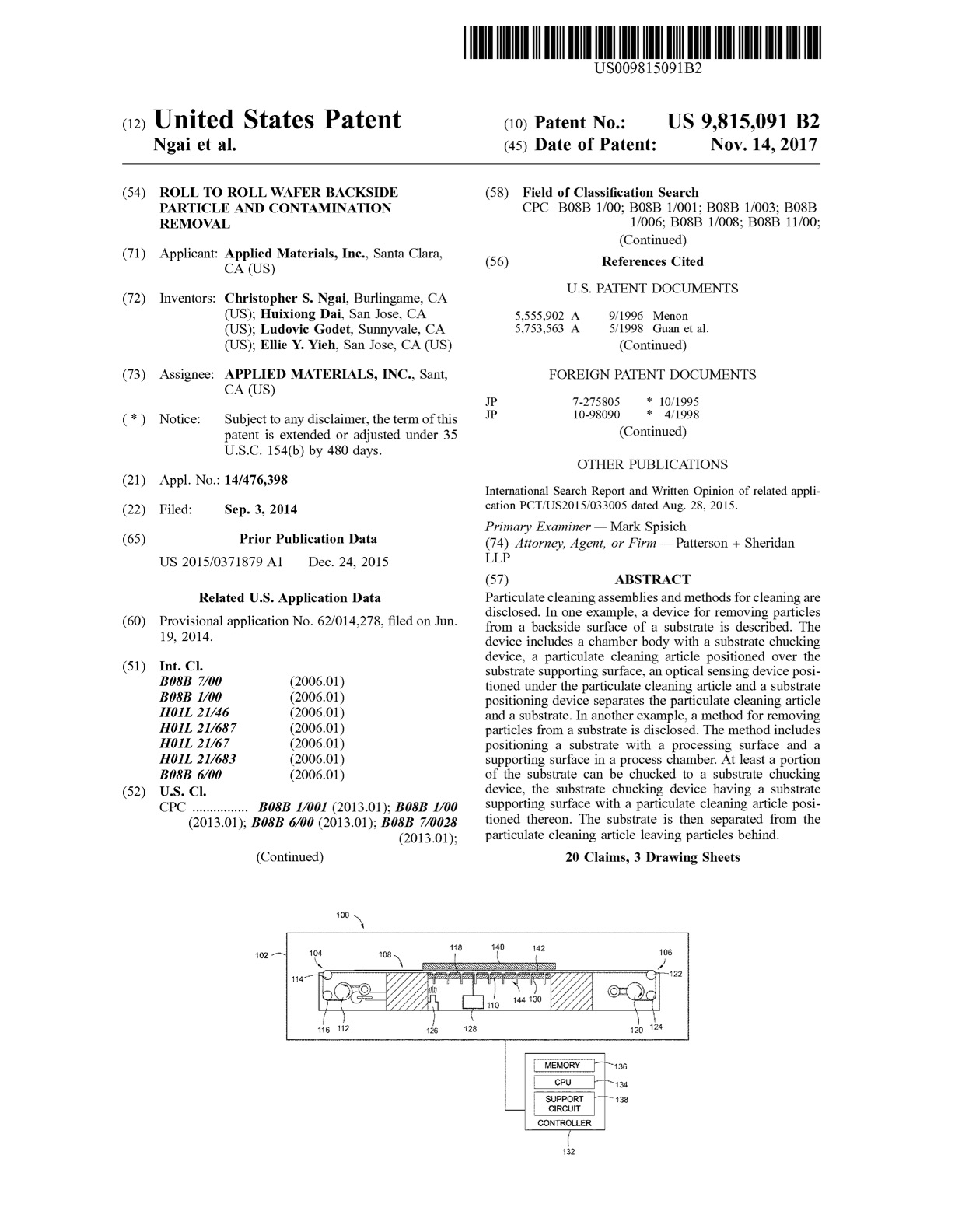
Ludovic Godet2022-01-07T00:26:57-05:00 US 9,815,091: Roll to roll wafer backside particle and contamination removal
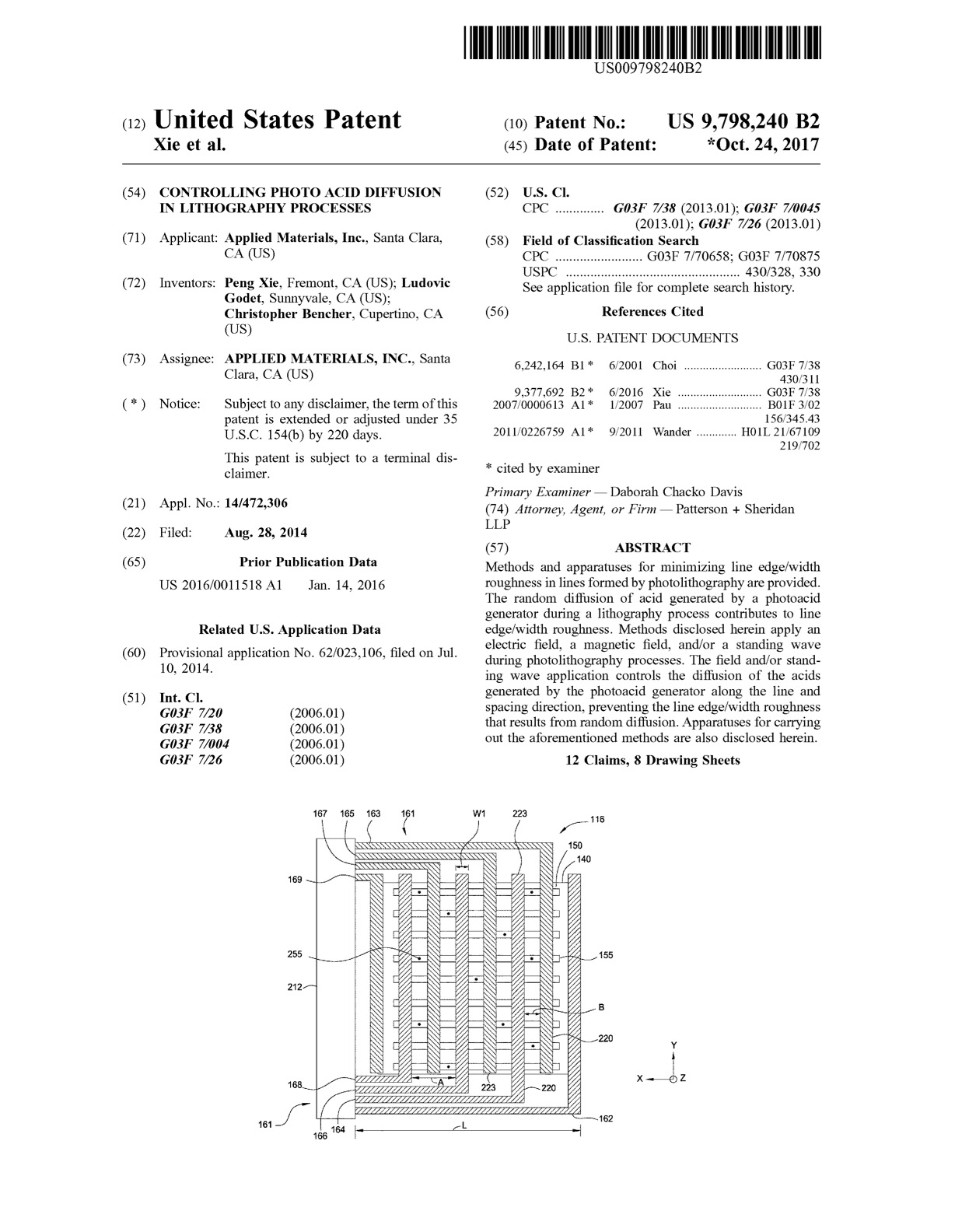
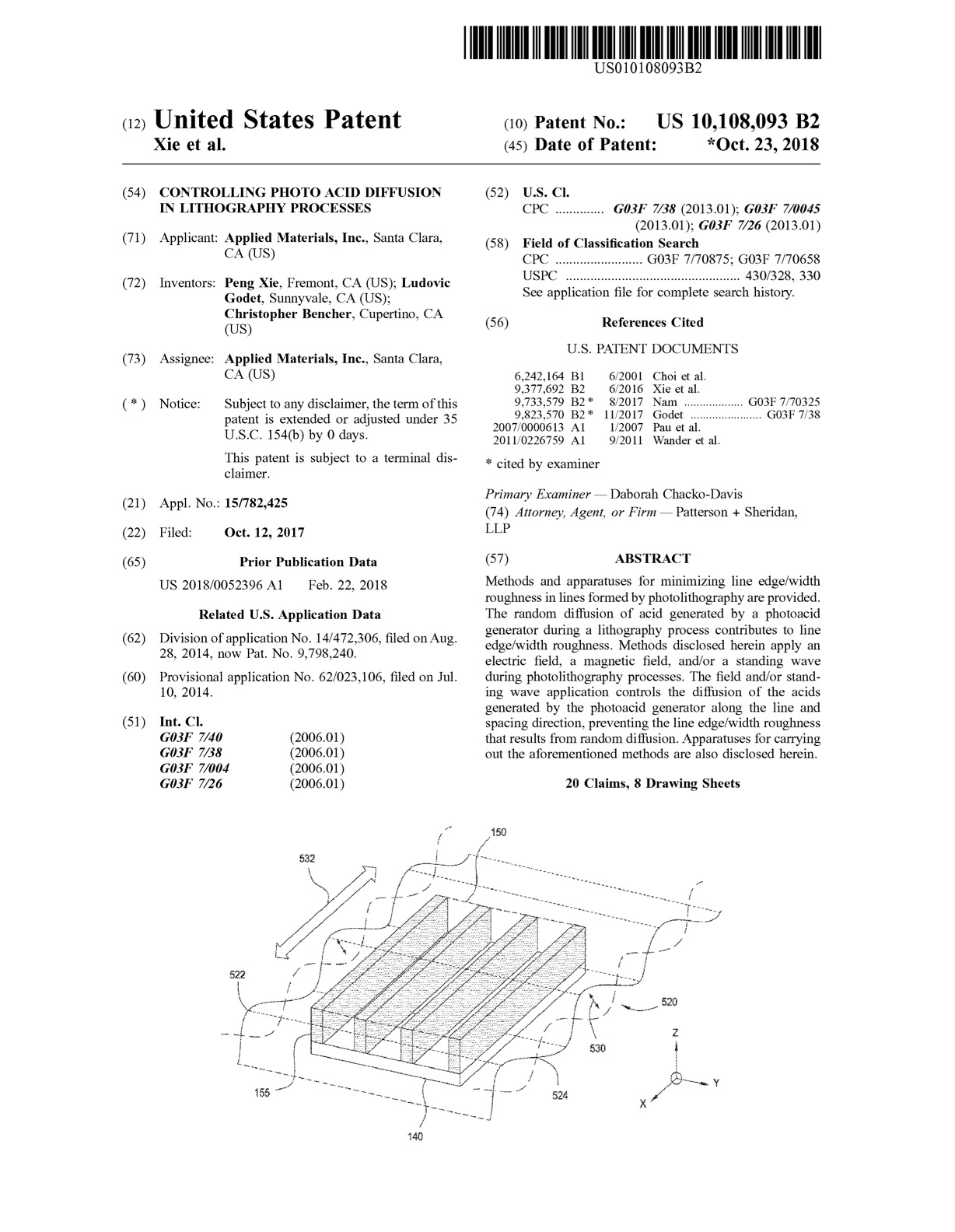
Ludovic Godet2022-01-05T02:05:04-05:00 US 9,798,240: Controlling photo acid diffusion in lithography processes
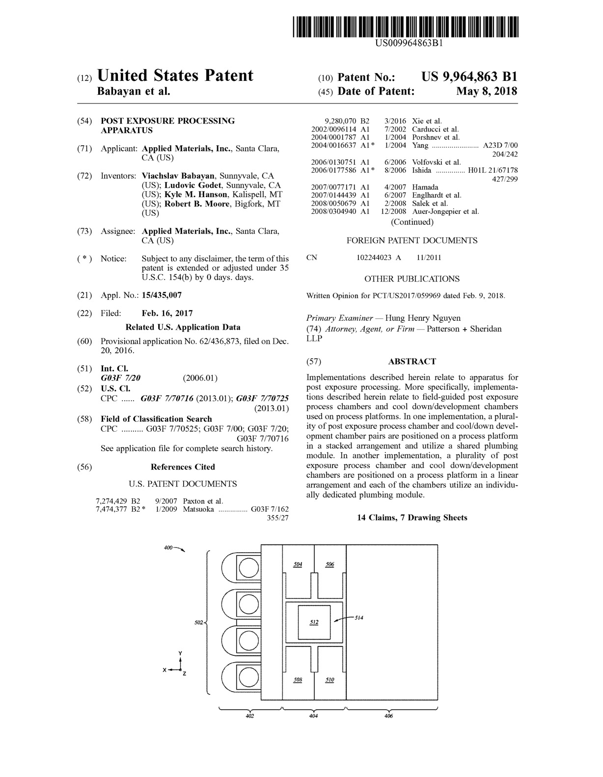
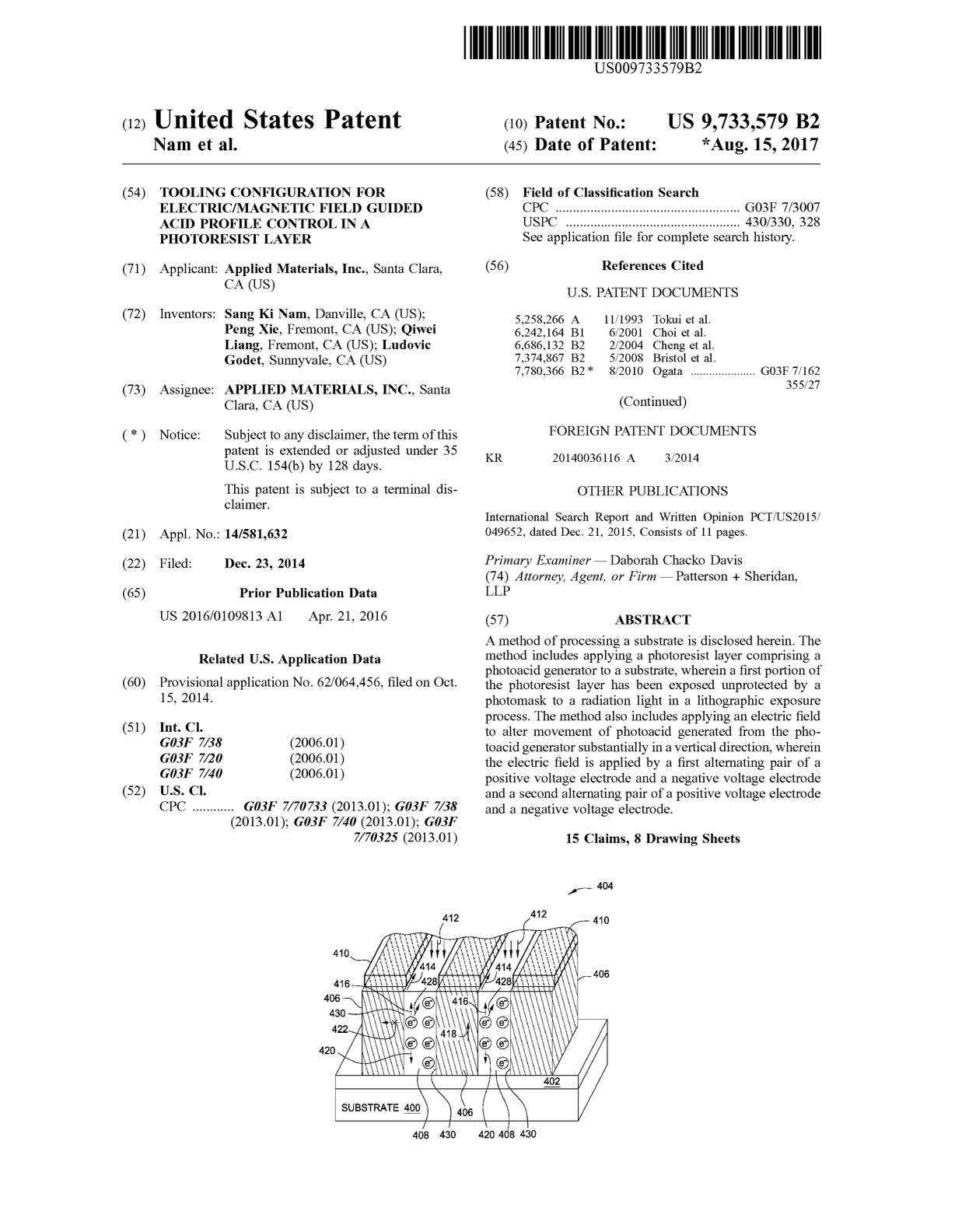
Ludovic Godet2022-01-05T01:31:08-05:00 US 9,733,579: Tooling Configuration for Electric/Magnetic Field Guided Acid Profile Control in PhotoResist Layer
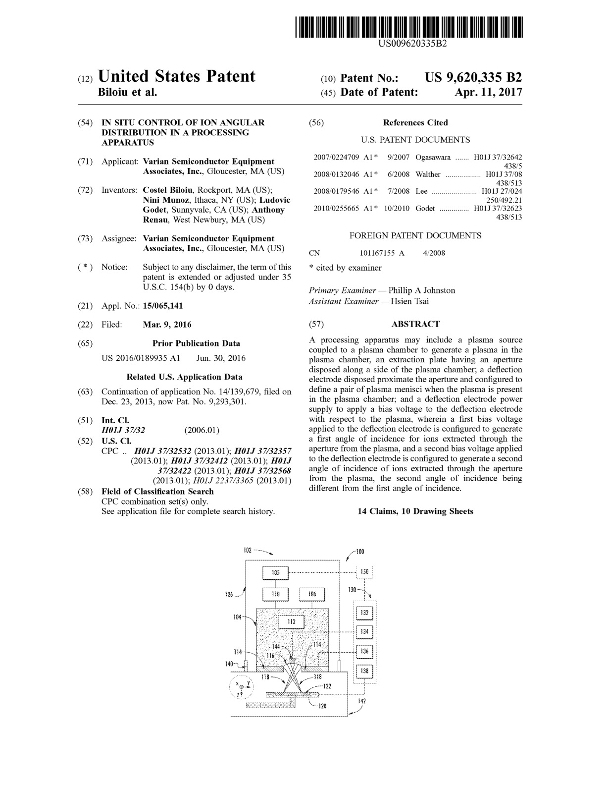
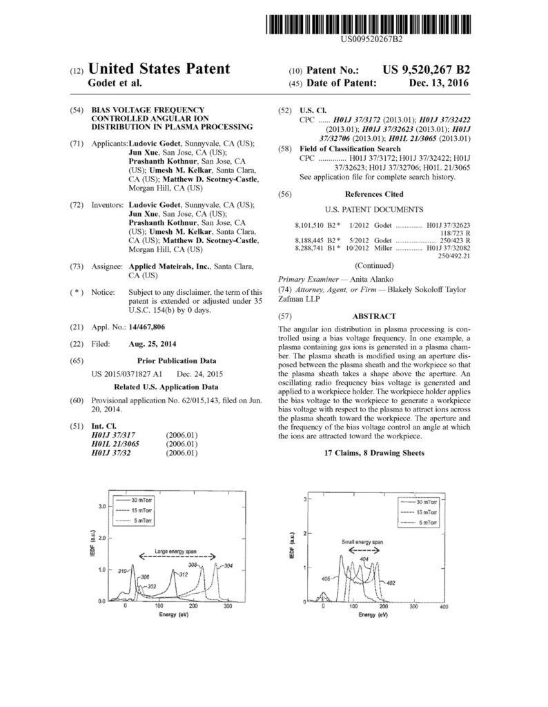
Ludovic Godet2022-01-05T00:58:46-05:00 US 9,620,335: In-situ Control of Ion Angular Distribution in a Processing Apparatus
Staff2021-01-31T18:33:30-05:00 US 9,515,166: Selective Atomic Layer Deposition Process Utilizing Patterned Self-Assembled Monolayers for 3D Structure Semiconductor Applications
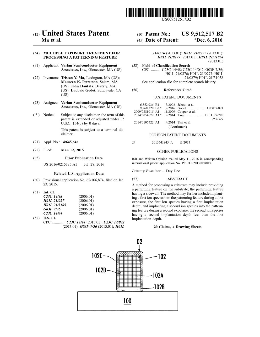
Staff2021-01-31T19:25:57-05:00 US 9,512,517: Multiple Exposure Treatment for Processing a Patterning Feature
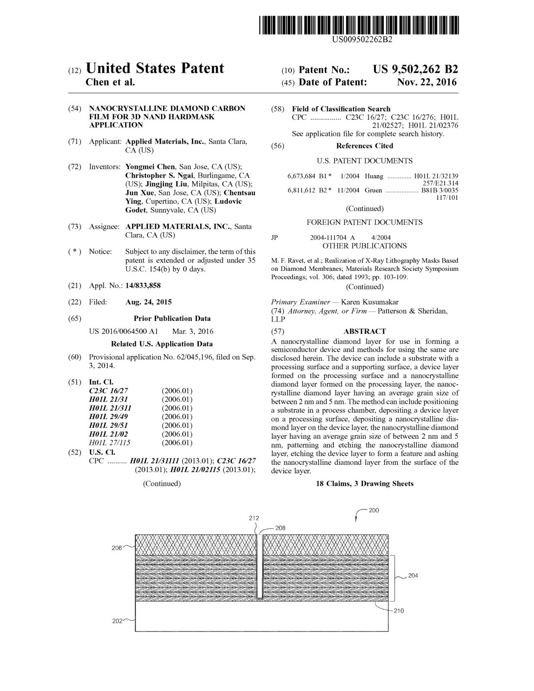
Staff2021-01-31T19:24:49-05:00 US 9,502,262: Nanocrystalline Diamond Carbon Film for 3D NAND Hardmask Application
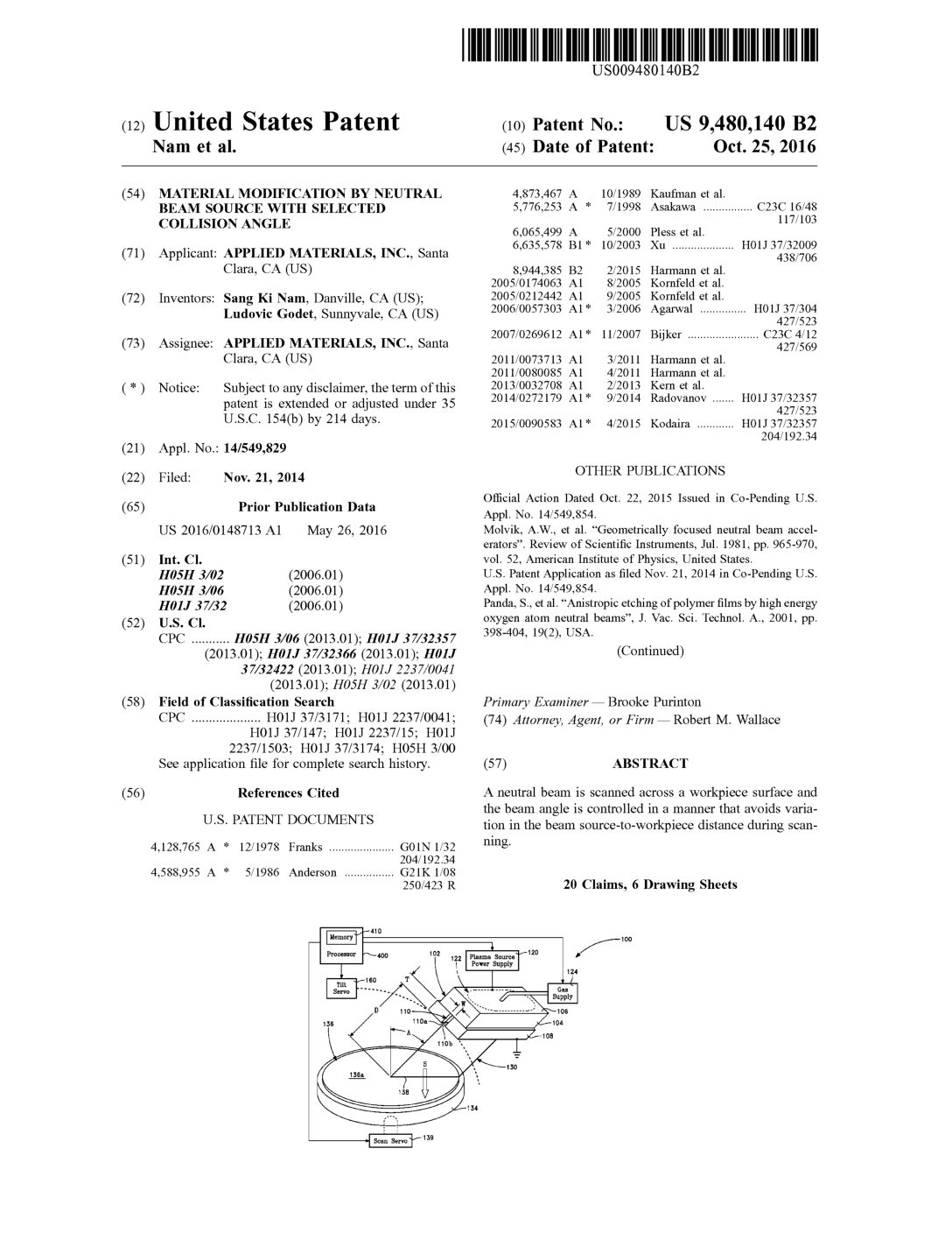
Staff2021-01-31T19:23:37-05:00 US 9,480,140: Material Modification by Neutral Beam Source with Selected Collision Angle
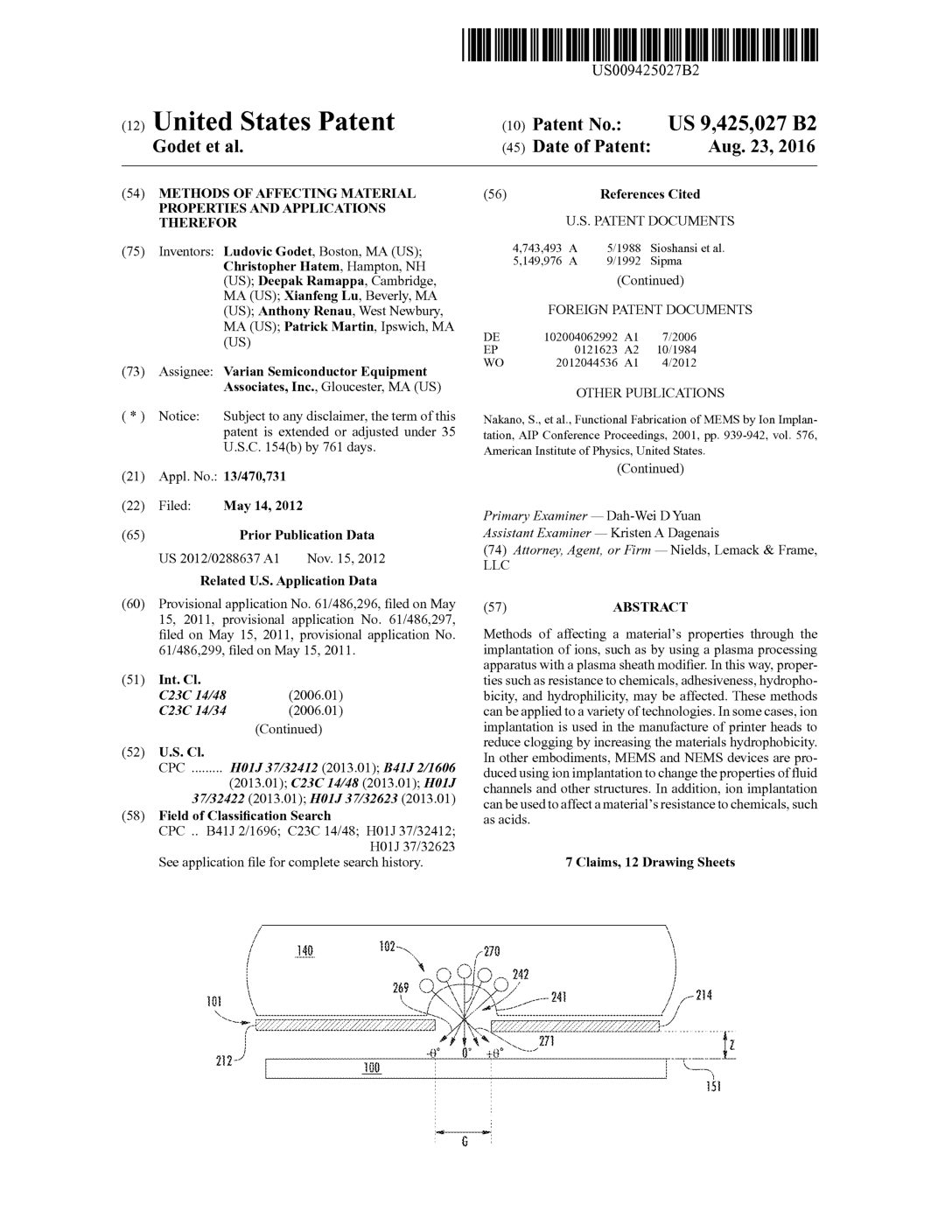
Staff2021-01-31T19:18:41-05:00 US 9,425,027: Methods of Affecting Material Properties and Applications
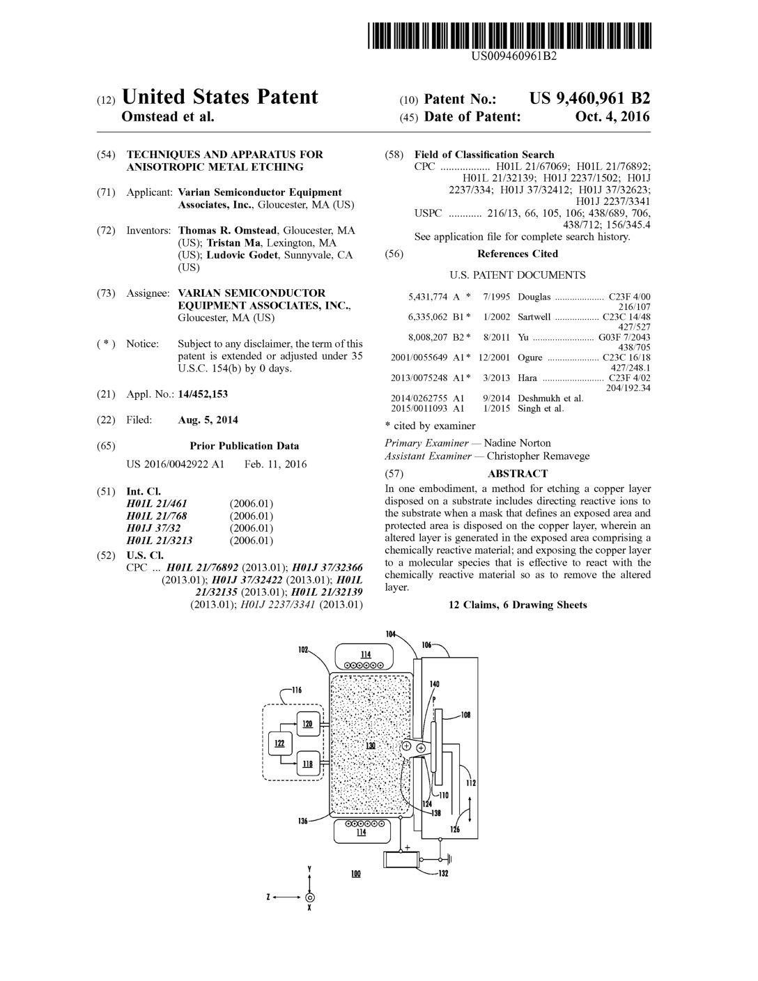
Staff2021-01-31T19:17:36-05:00 US 9,412,613: Development of High Etch Selectivity Hardmask by Ion Implantation in Carbon Films
Staff2021-01-31T19:10:44-05:00 US 9,382,625: Remote Plasma Source Based Cyclic CVD Process for Nanocrystalline Diamond Deposition
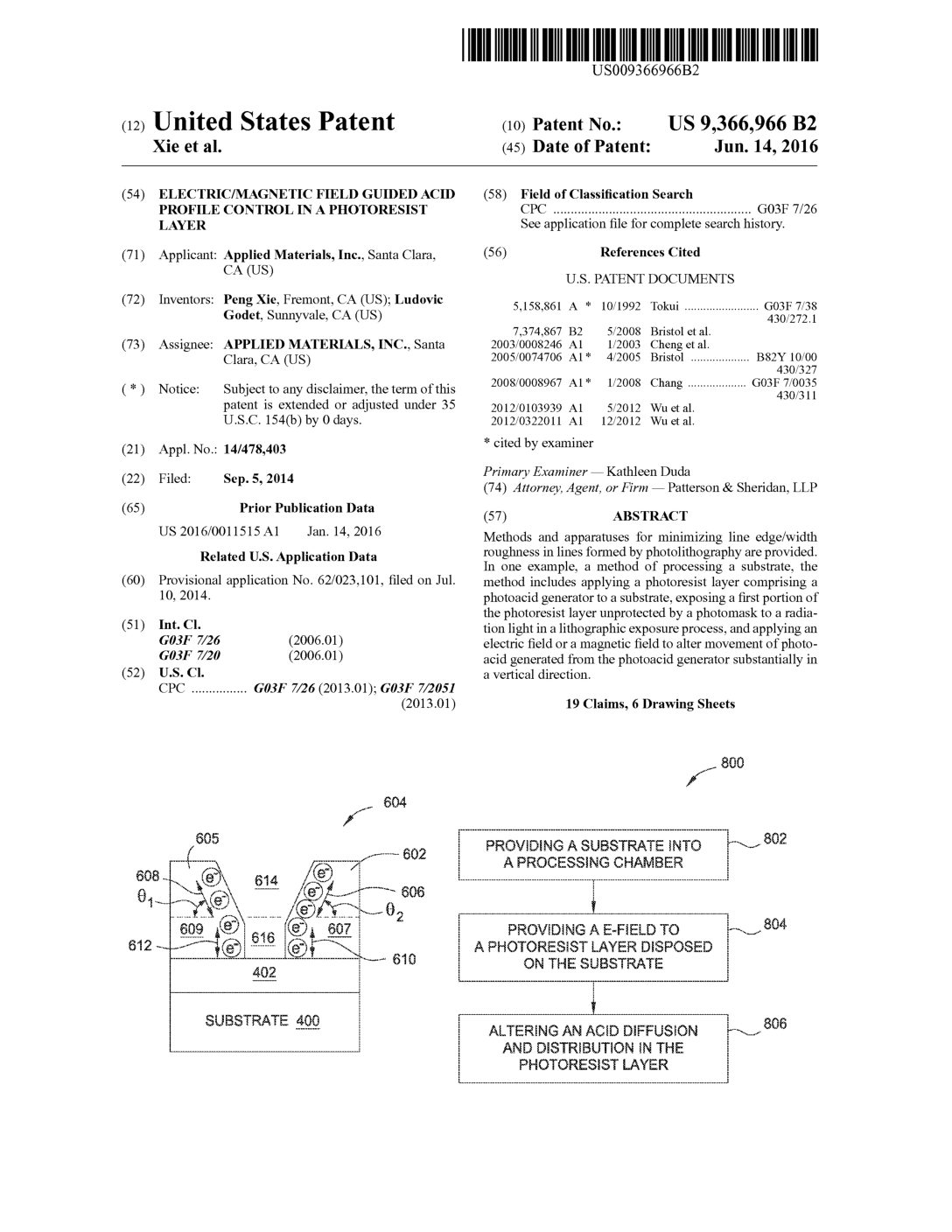
Staff2021-01-31T19:06:53-05:00 US 9,366,966: Electric/magnetic Field Guided Acid Profile Control in a Photoresist Layer
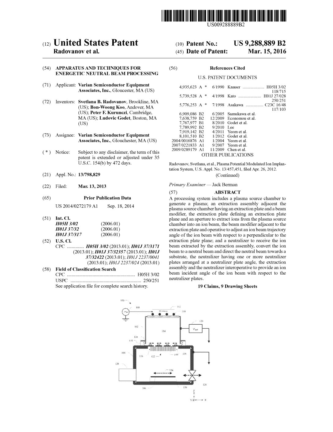
Staff2021-01-31T19:02:05-05:00 US 9,288,889: Apparatus and Techniques for Energetic Neutral Beam Processing
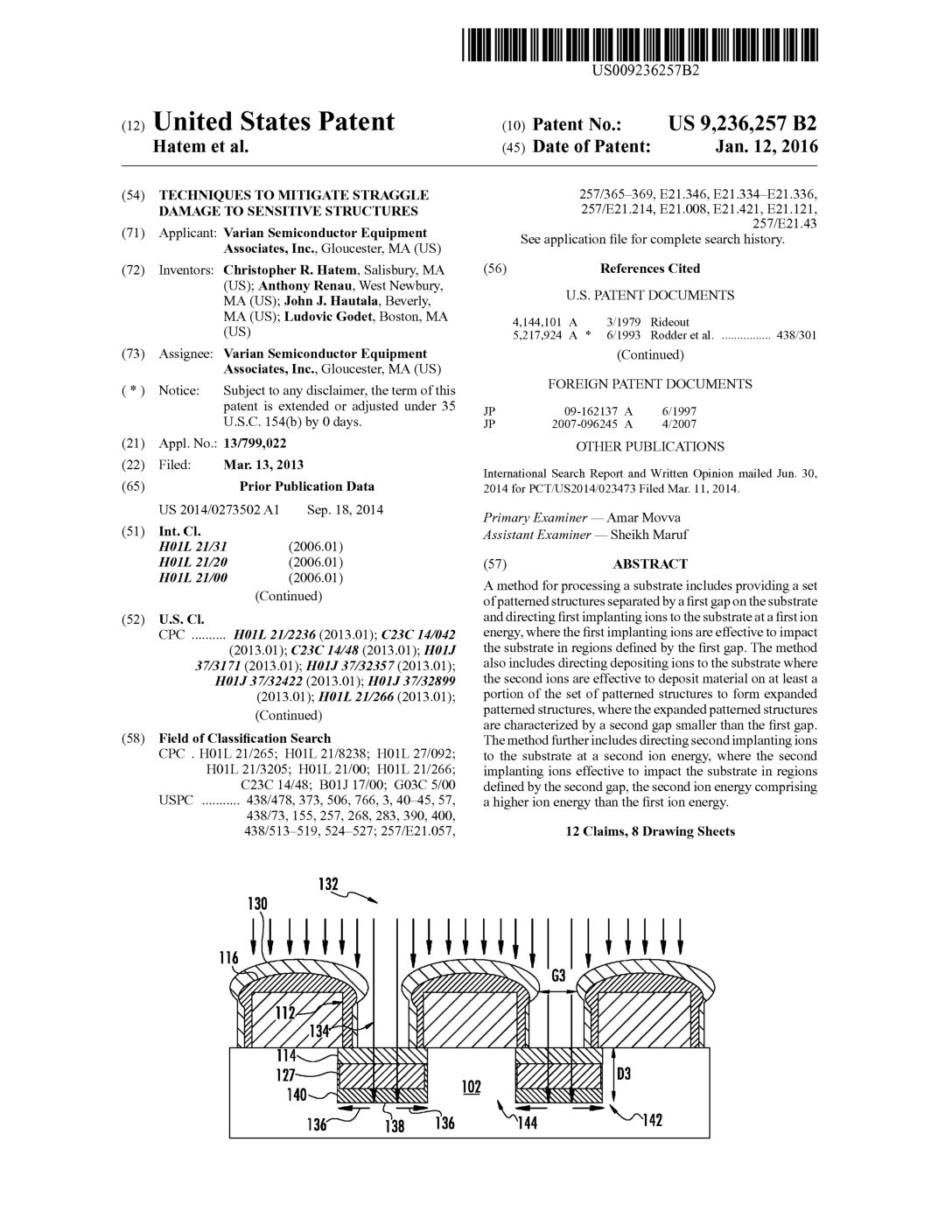
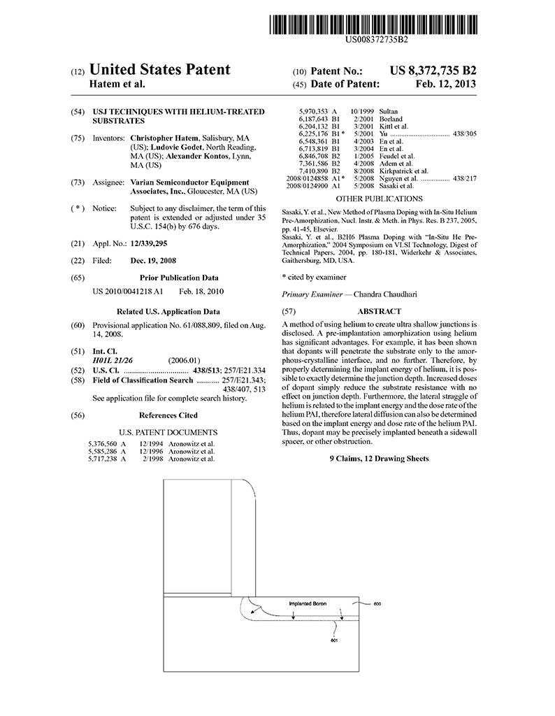
Staff2021-01-31T18:56:21-05:00 US 9,236,257: Techniques to Mitigate Straggle Damage to Sensitive Structures
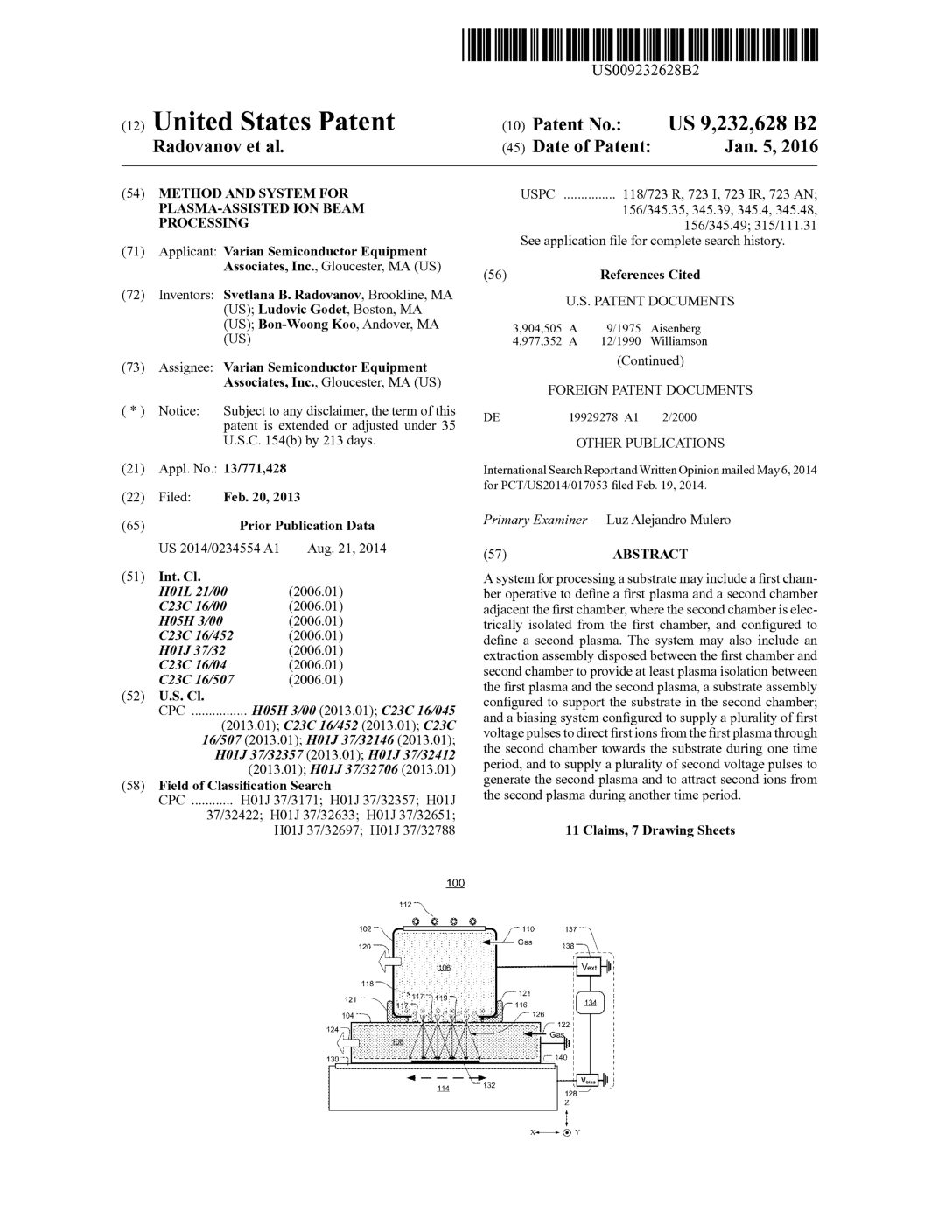
Staff2021-01-31T18:55:14-05:00 US 9,232,628: Method and System for Plasma –Assisted Ion Beam Processing
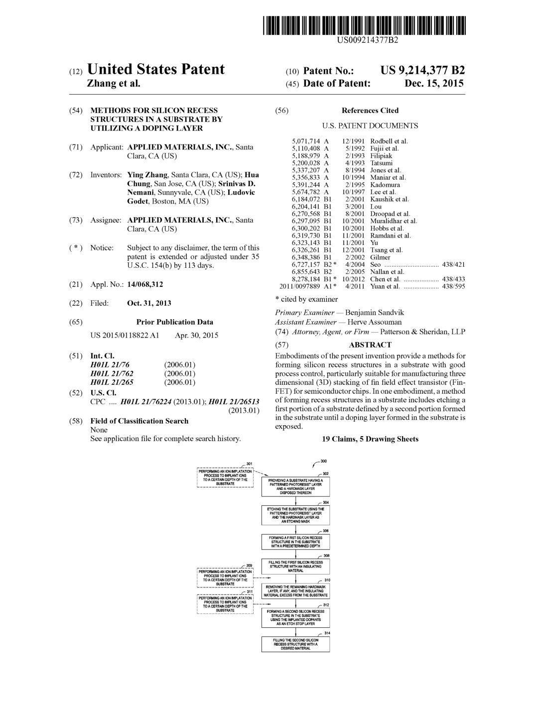
Staff2021-01-31T18:54:16-05:00 US 9,214,377: Methods for Silicon Recess Structure in a Substrate by Utilizing a Doping Layer
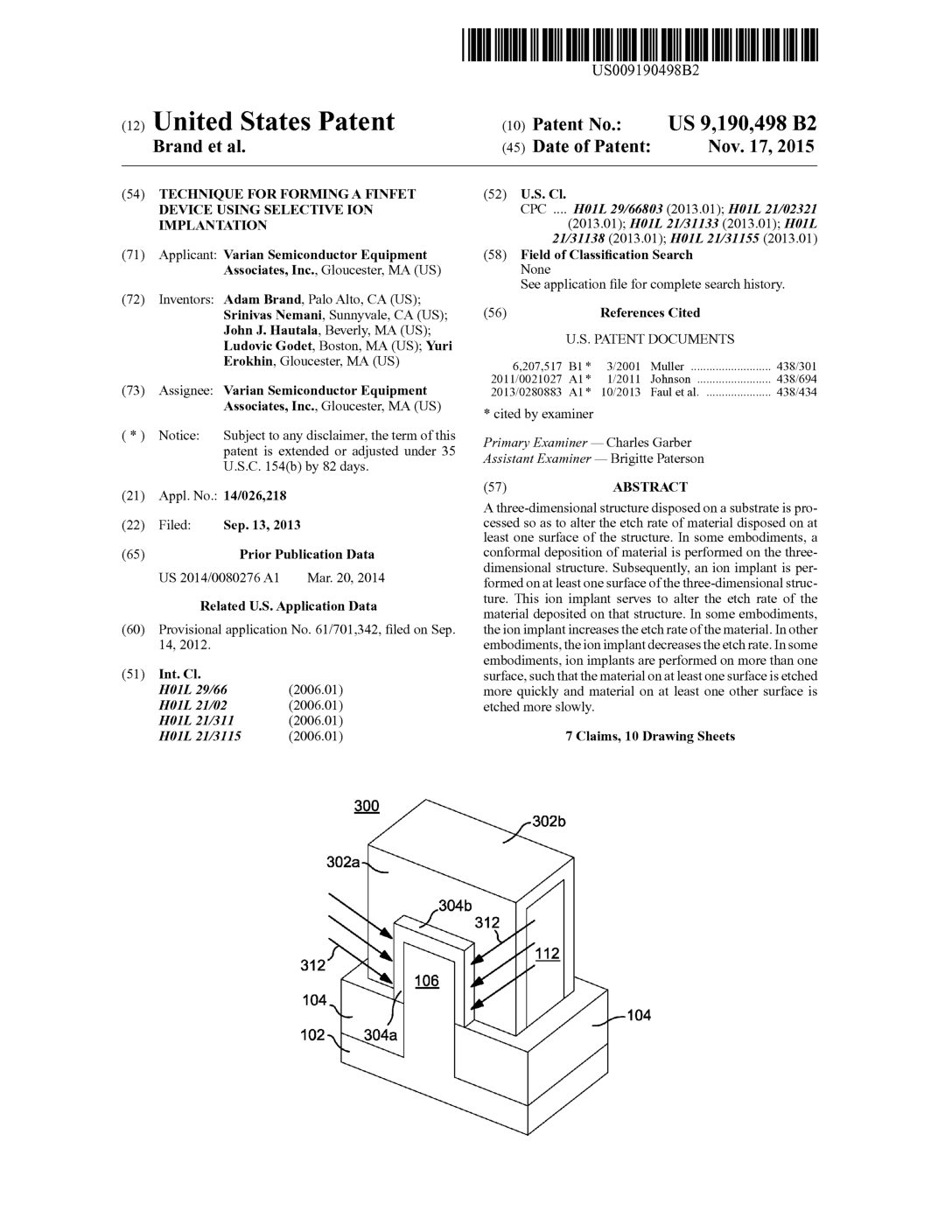
Staff2021-01-31T18:52:41-05:00 US 9,190,498: Technique for Forming a FinFET Device using Selective Ion Implantation
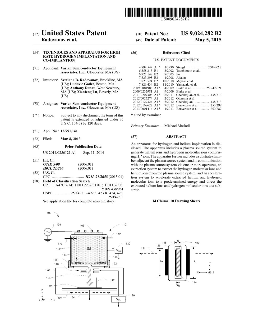
Staff2021-02-01T11:19:08-05:00 US 9,024,282: Techniques and Apparatus for High Rate Hydrogen Implantation and Co-implant
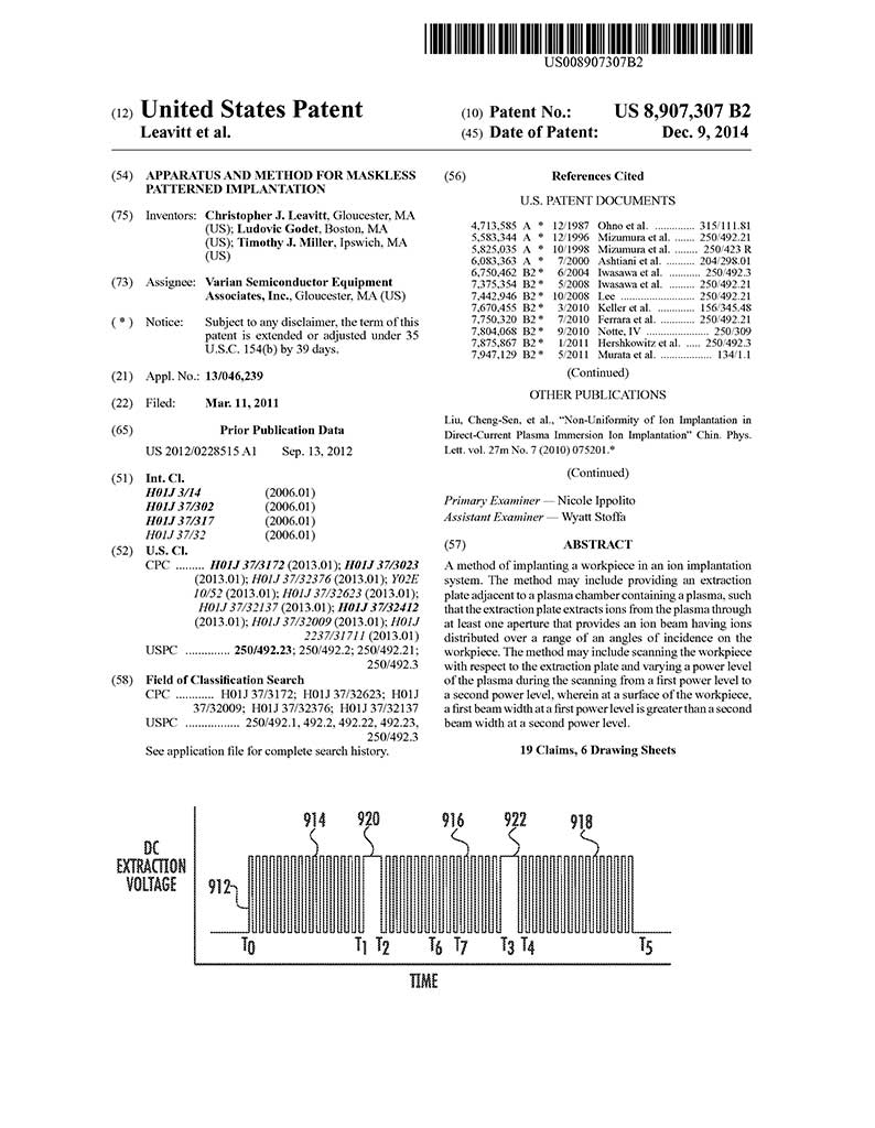
Staff2021-02-03T11:39:05-05:00 US 8,907,307: Apparatus and Method for Maskless Patterned Implantation
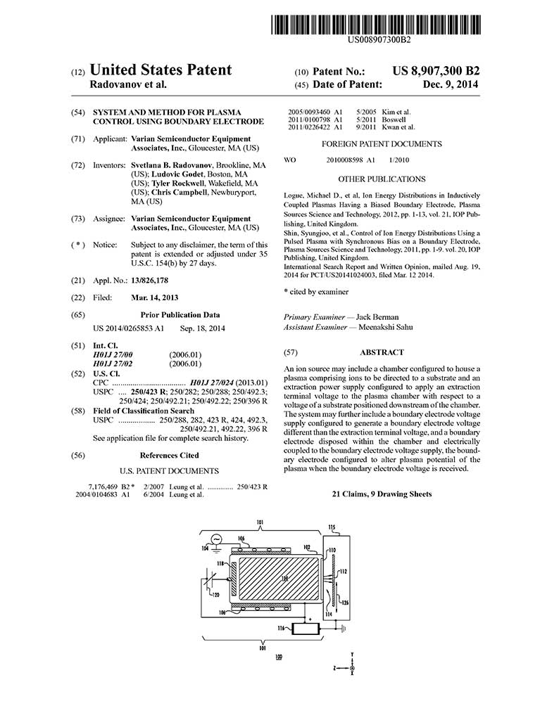
Staff2021-02-05T10:42:54-05:00 US 8,907,300: System and Method for Plasma Control Using Boundary Electrode
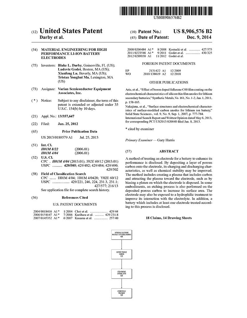
Staff2021-02-03T11:59:40-05:00 US 8,906,576: Material Engineering for High Performance Li-ion Battery Electrodes
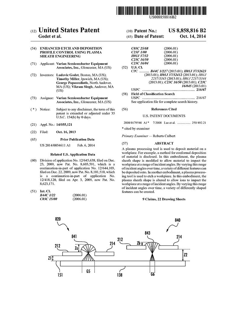
Staff2021-02-04T11:26:34-05:00 US 8,858,816: Enhanced Etch and Deposition Profile Control Using Plasma Sheath Engineering
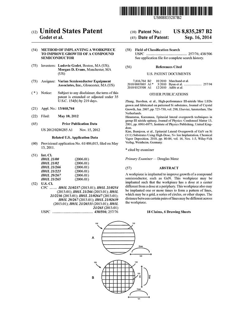
Staff2021-02-03T11:49:45-05:00 US 8,835,287: Method of Implanting a Workpiece to Improve Growth of a Compound Semiconductor
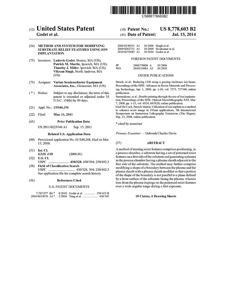
Staff2021-02-04T11:14:27-05:00 US 8,778,603: Method and System for Modifying Substrate Relief Features Using Ion Implantation
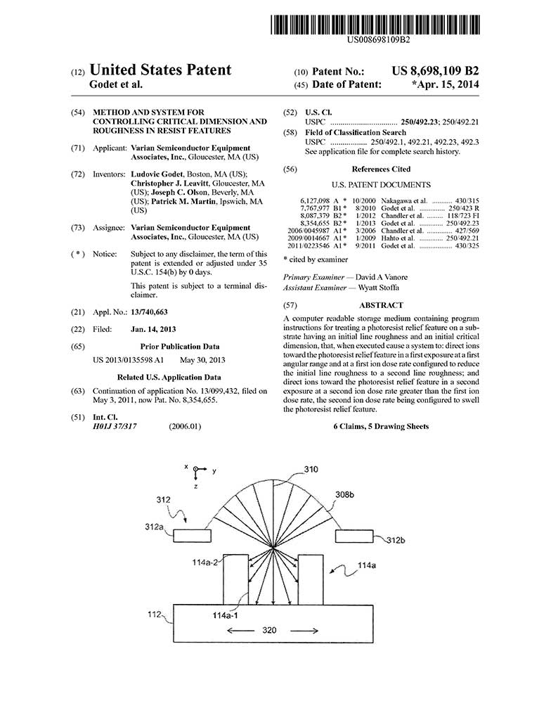
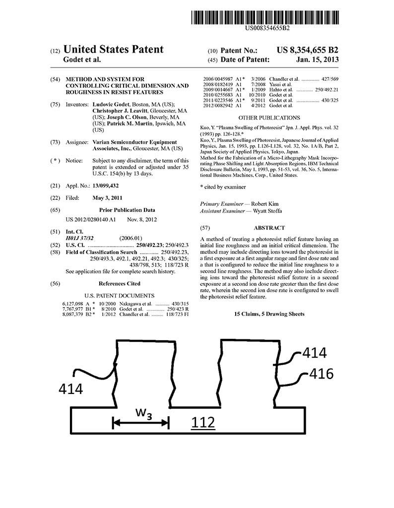
Staff2021-02-04T11:10:37-05:00 US 8,698,109: Method and System for Controlling Critical Dimension and Roughness in Resist Features
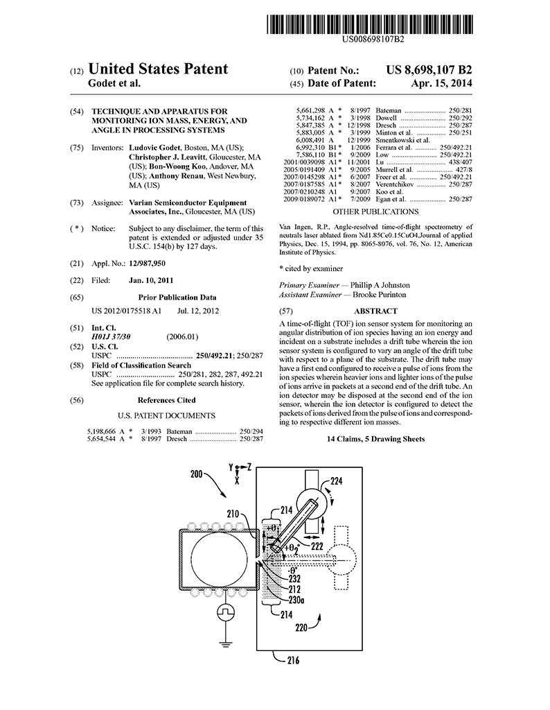
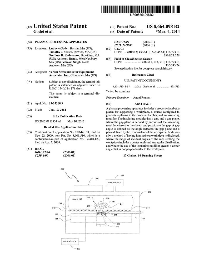
Staff2021-02-05T12:09:53-05:00 US 8,698,107: Technique and Apparatus for Monitoring Ion Mass, Energy, and Angle in Processing Systems
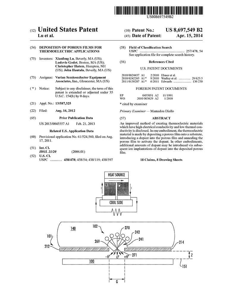
Staff2021-02-02T15:41:12-05:00 US 8,697,549: Deposition of Porous Films for Thermoelectric Applications
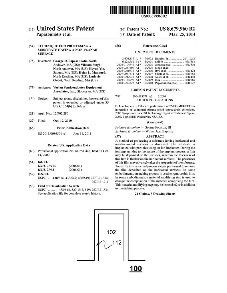
Staff2021-02-04T11:51:09-05:00 US 8,679,960: Technique for Processing a Substrate Having a Non-planar Surface
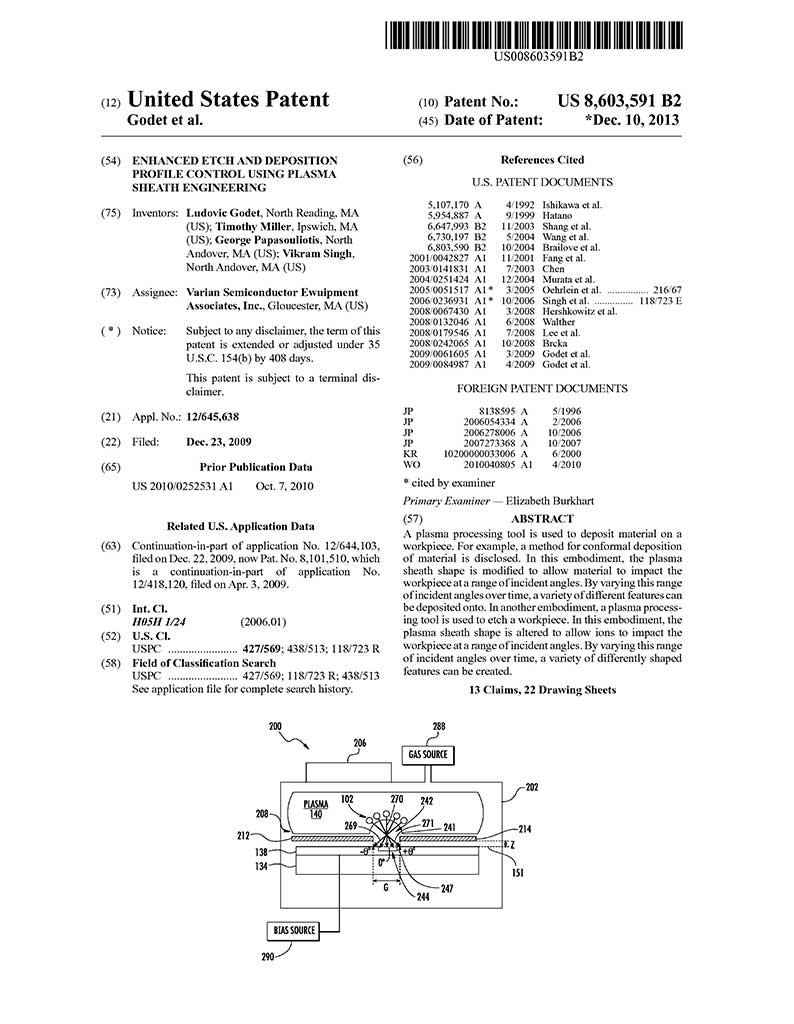
Staff2021-02-04T11:18:33-05:00 US 8,603,591: Enhanced Etch and Deposition Profile Control using Plasma Sheath Engineering
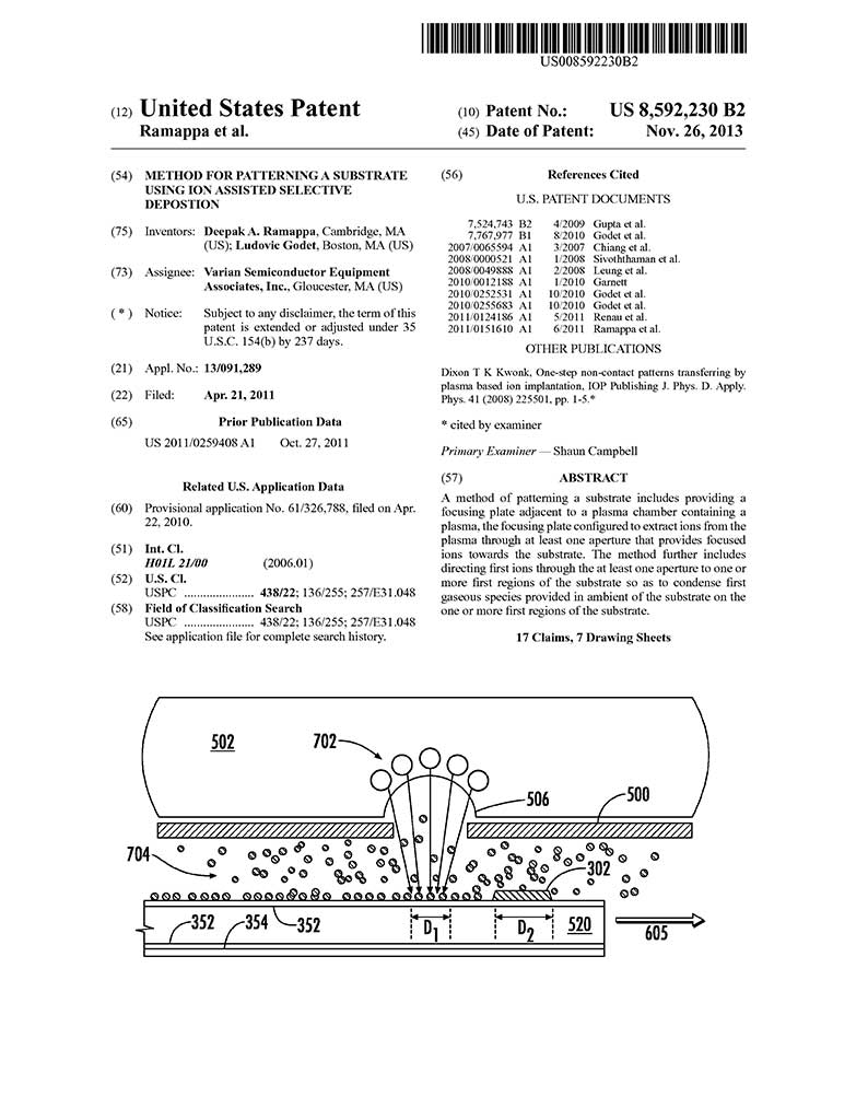
Staff2021-02-05T12:43:25-05:00 US 8,592,230: Method for patterning a substrate using ion assisted selective deposition
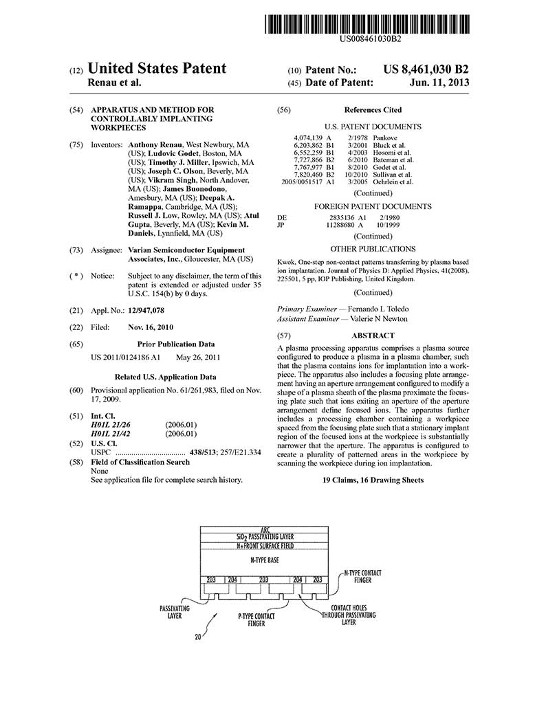
Staff2021-02-03T11:27:38-05:00 US 8,461,030: Apparatus and method for controllably implanting workpieces
Staff2021-02-04T11:06:17-05:00 US 8,460,569: Method and system for post-etch treatment of patterned substrate features
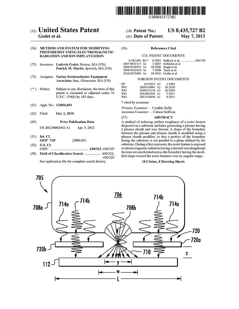
Staff2021-02-03T12:18:41-05:00 US 8,435,727: Method and system for modifying photoresist using electromagnetic radiation and ion implantation
Staff2021-02-03T12:14:09-05:00 US 8,354,655: Method and System for Controlling Critical Dimension and Roughness in Resist Features
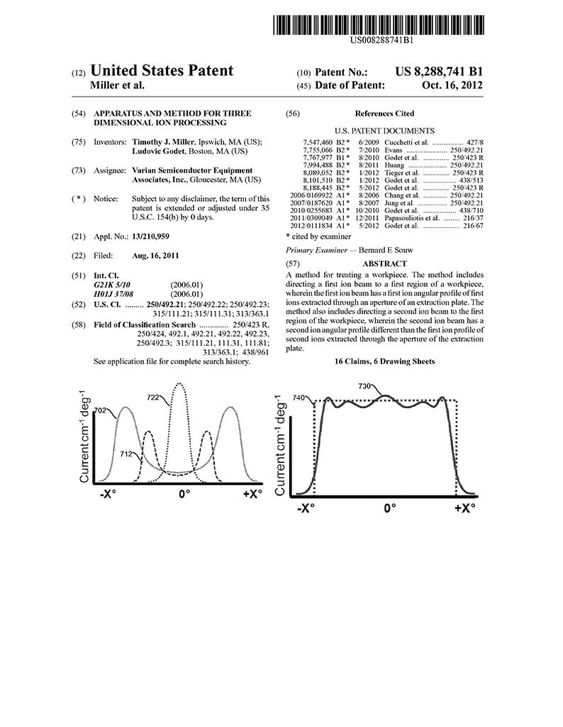
Staff2021-02-05T12:39:42-05:00 US 8,288,741: Apparatus and Method for Three Dimensional Ion Processing
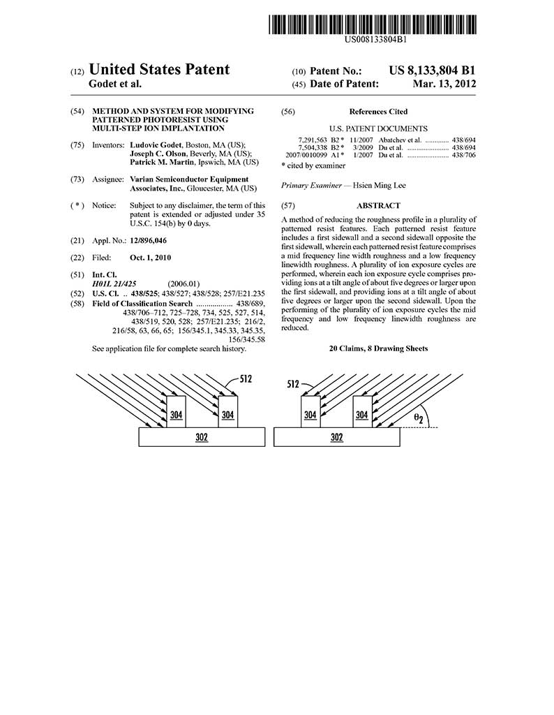
Staff2021-02-03T12:09:26-05:00 US 8,133,804: Method and system for modifying patterned photoresist using multi-step ion implantation
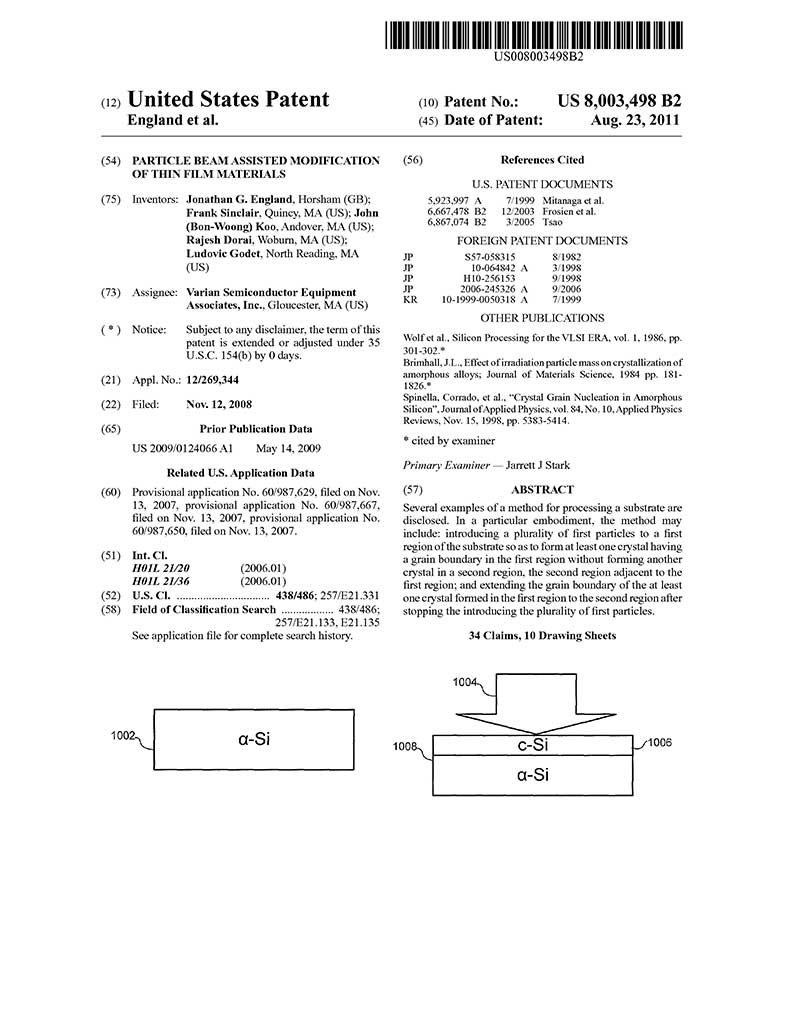
Staff2021-02-02T15:37:21-05:00 US 8,003,498: Particle Beam Assisted Modification of Thin Film Materials
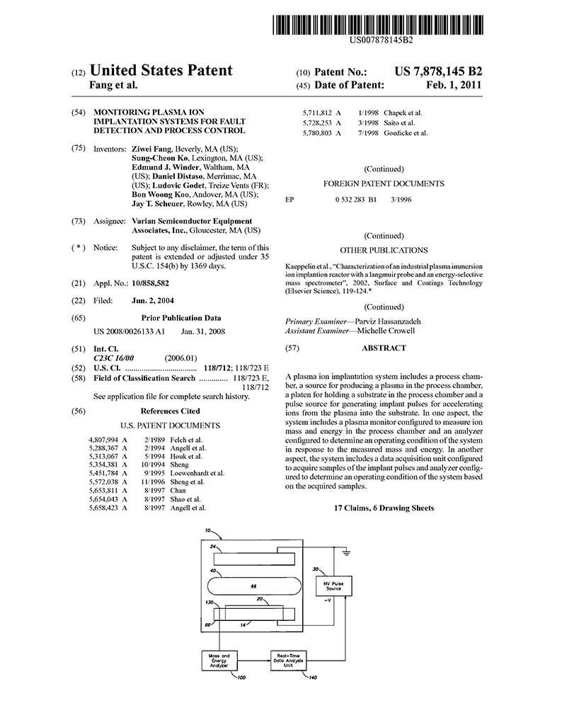
Staff2021-02-05T12:03:37-05:00 US 7,878,145 : Monitoring plasma ion implantation systems for fault detection and process control
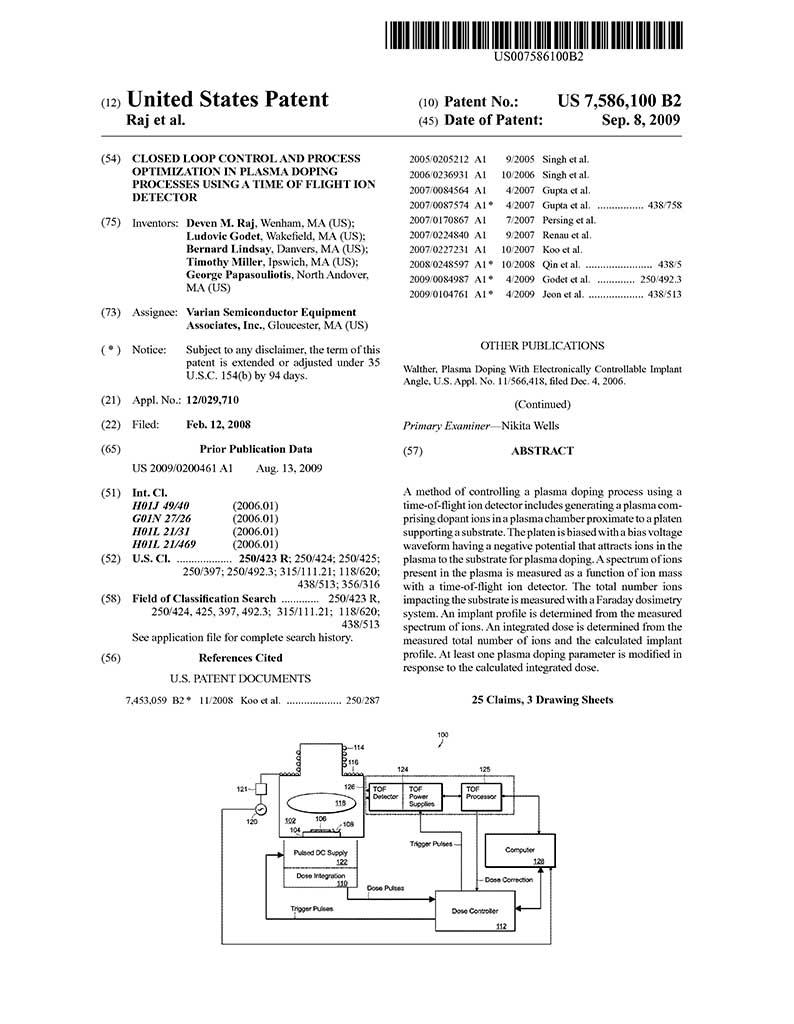
Staff2021-02-05T10:56:15-05:00 US 7,856,100 B2: Closed Loop Control and Process Optimization in Plasma Doping Processes Using Time Of Flight Ion Detector
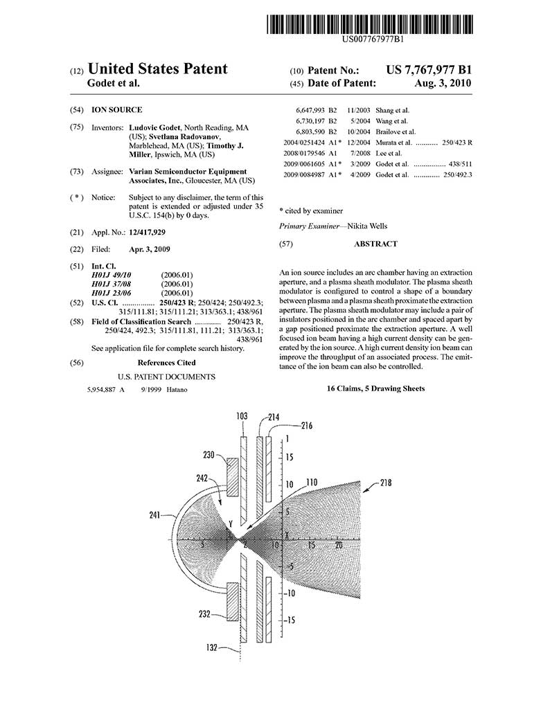
Staff2021-02-05T10:52:09-05:00 US 7,476,849: Technique for monitoring and controlling a plasma process
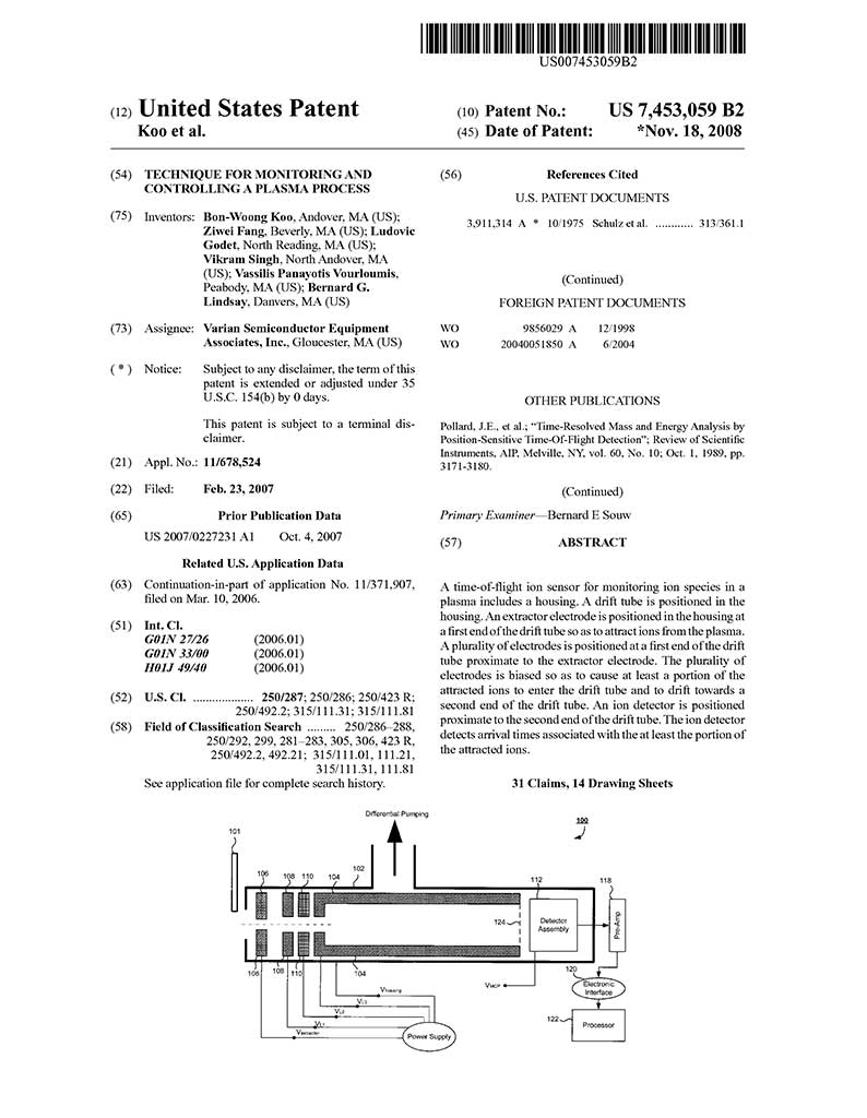
Staff2021-02-05T10:48:20-05:00 US 7,453,059: Technique for monitoring and controlling a plasma process
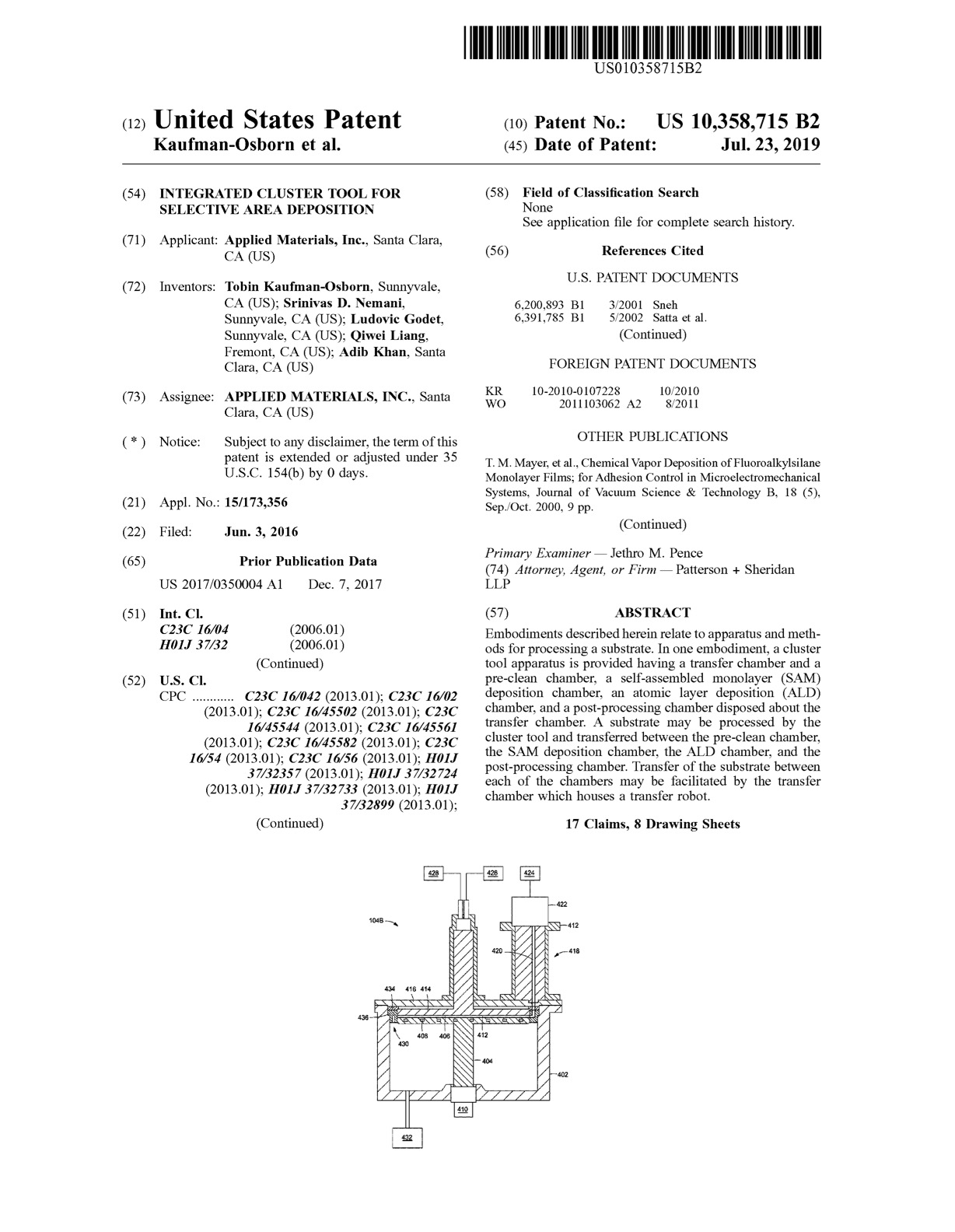
Ludovic Godet2022-01-10T14:29:45-05:00 US 10,358,715: Integrated cluster tool for selective area deposition
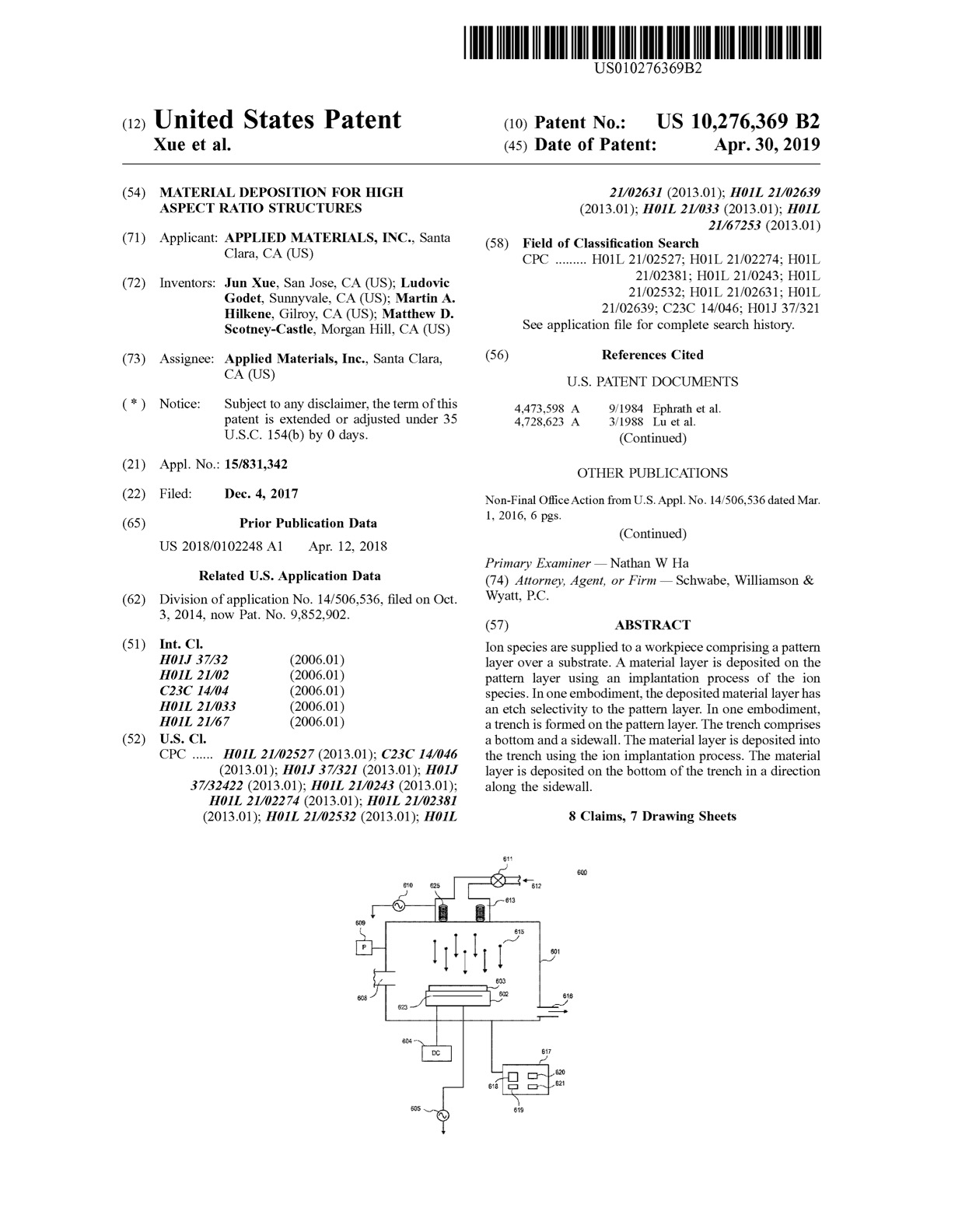
Ludovic Godet2022-01-10T14:22:05-05:00 US 10,276,369: Material deposition for high aspect ratio structures
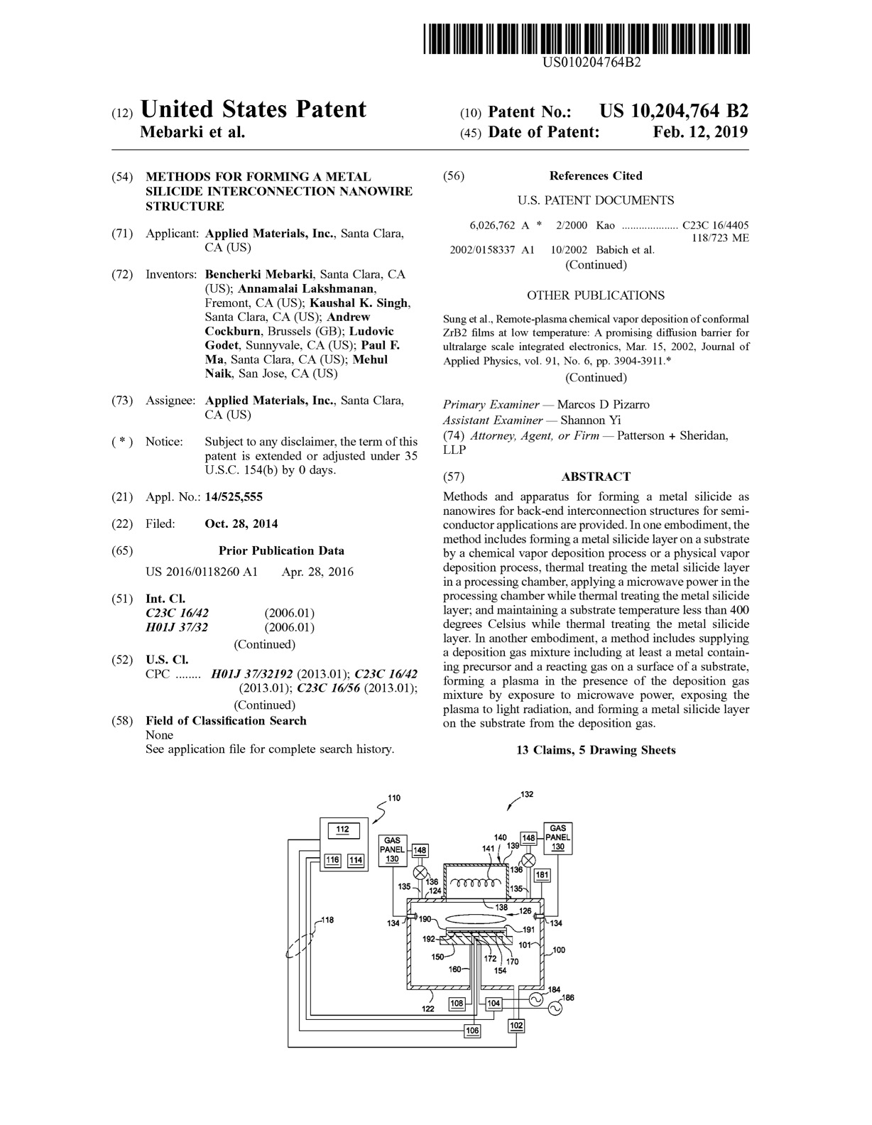
Ludovic Godet2022-01-10T14:16:23-05:00 US 10,204,764: Methods for forming a metal silicide interconnection nanowire structure
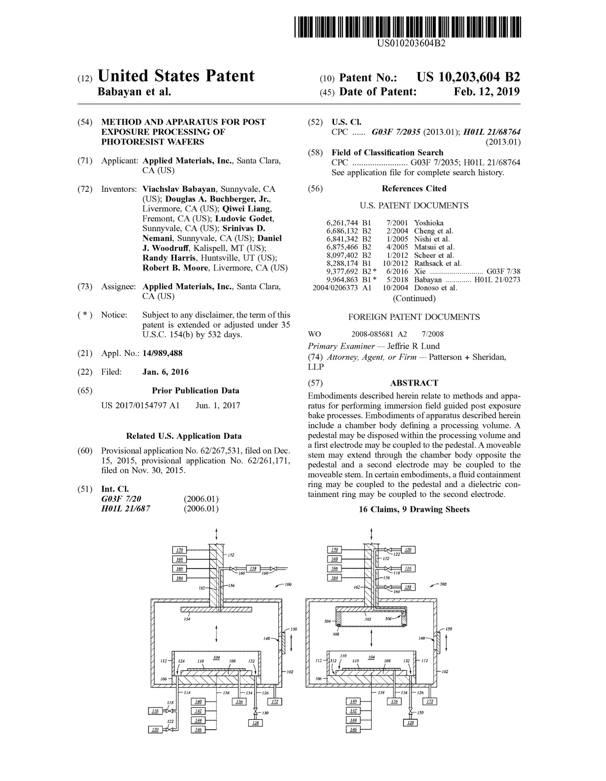
Ludovic Godet2022-01-10T13:35:28-05:00 US 10,203,604: Method and apparatus for post exposure processing of photoresist wafers
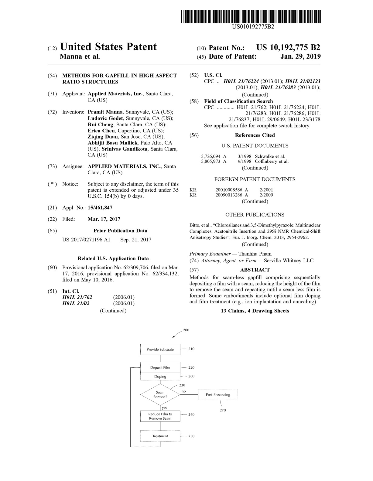
Ludovic Godet2022-01-10T13:31:49-05:00 US 10,192,775: Methods for gapfill in high aspect ratio structures
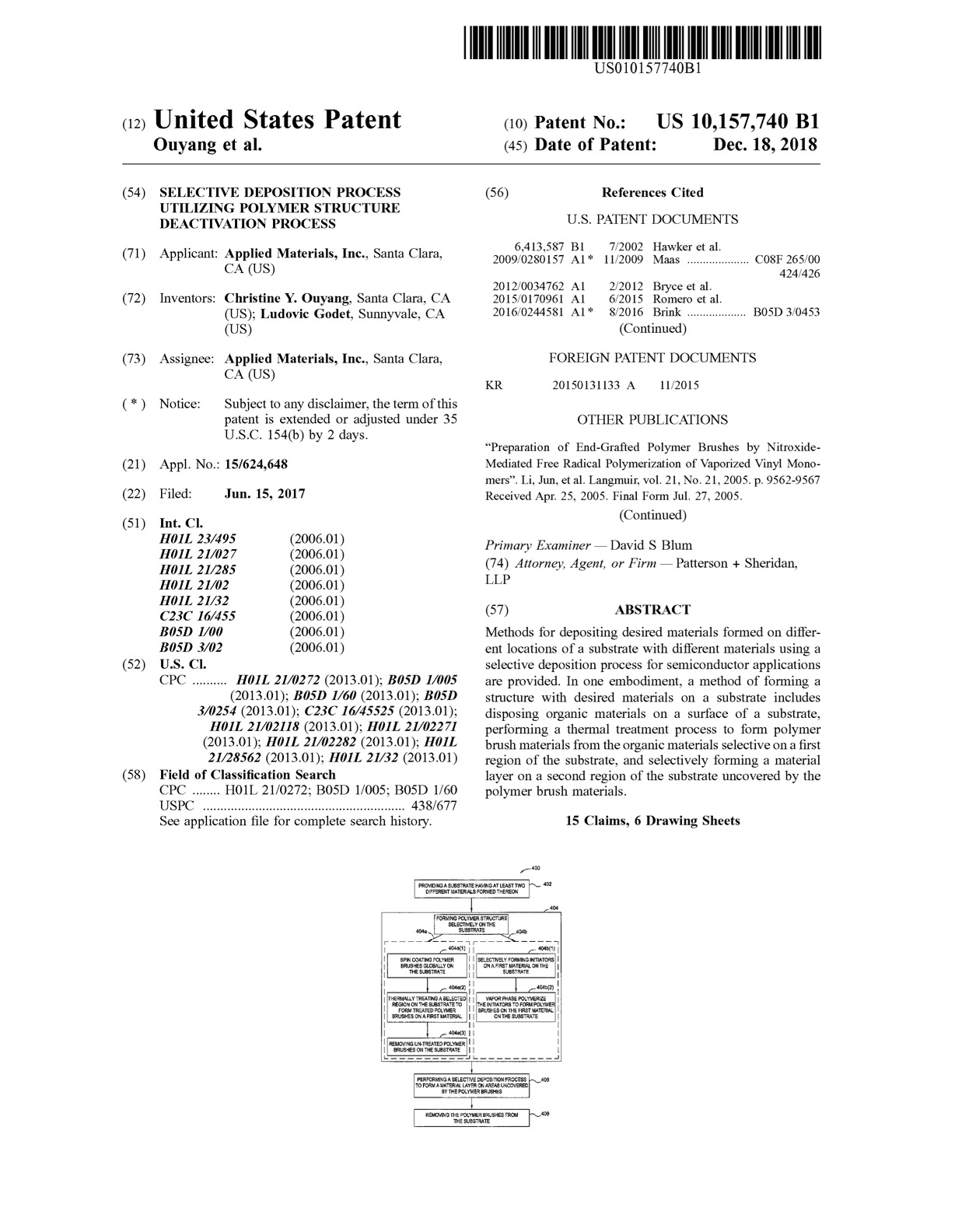
Ludovic Godet2022-01-10T13:24:12-05:00 US 10,157,740: Selective deposition process utilizing polymer structure deactivation process
Ludovic Godet2022-01-07T01:54:27-05:00 US 10,108,093: Controlling photo acid diffusion in lithography processes
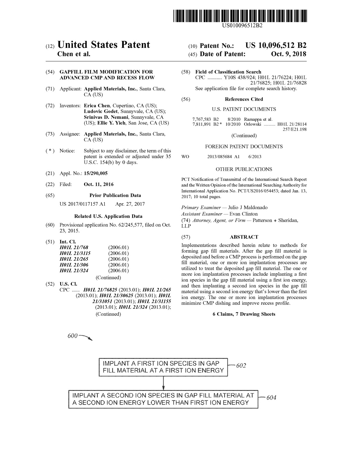
Ludovic Godet2022-01-07T01:48:01-05:00 US 10,096,512: Gapfill film modification for advanced CMP and recess flow
Ludovic Godet2022-01-07T01:39:53-05:00 US 10,048589: FGPEB application for photoresist microbridge defects,


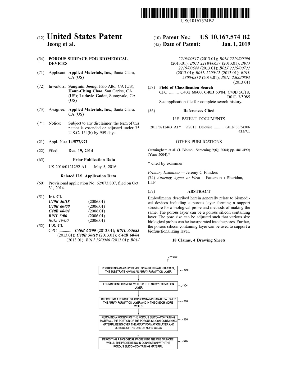

Social Media