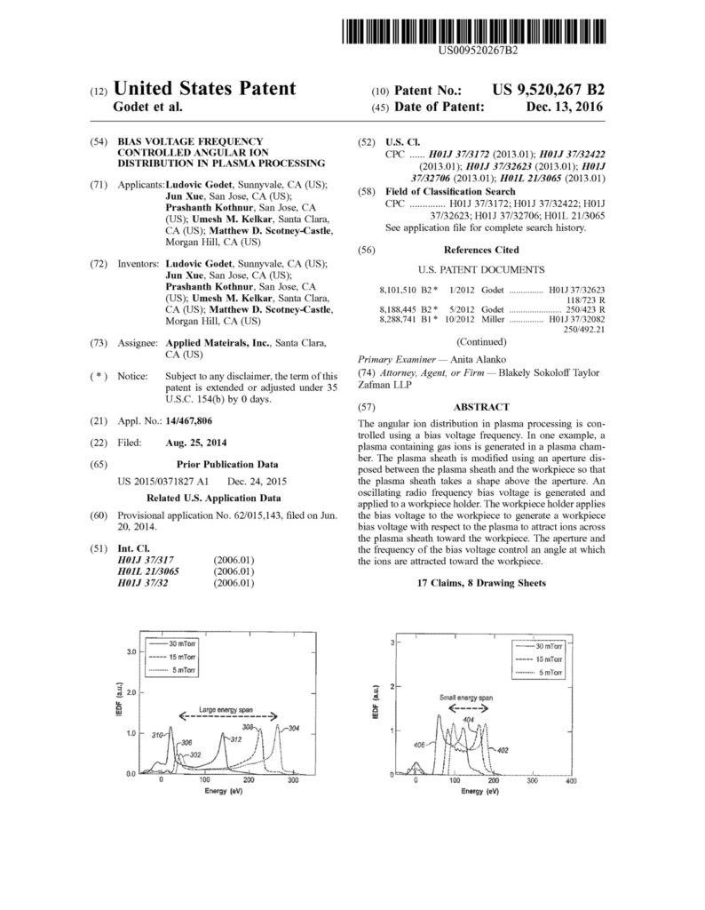
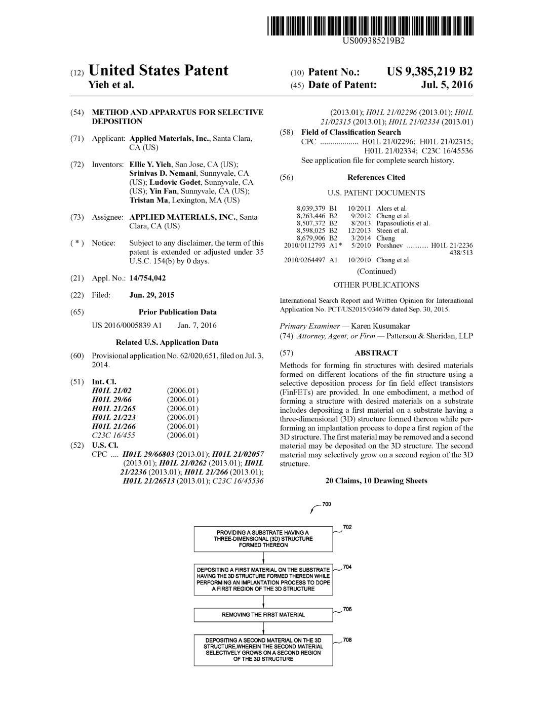
Staff2021-01-31T18:33:30-05:00 US 9,515,166: Selective Atomic Layer Deposition Process Utilizing Patterned Self-Assembled Monolayers for 3D Structure Semiconductor Applications
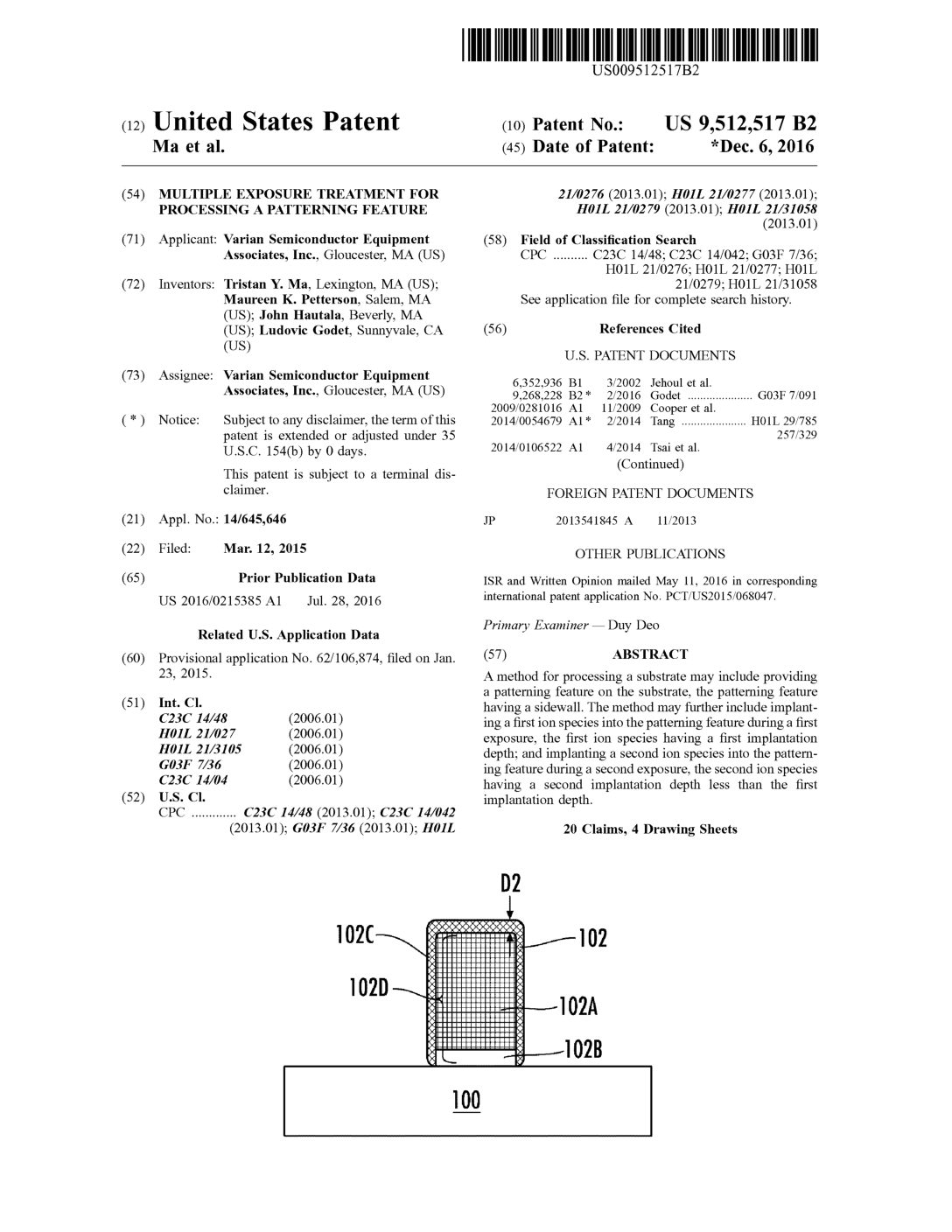
Staff2021-01-31T19:25:57-05:00 US 9,512,517: Multiple Exposure Treatment for Processing a Patterning Feature
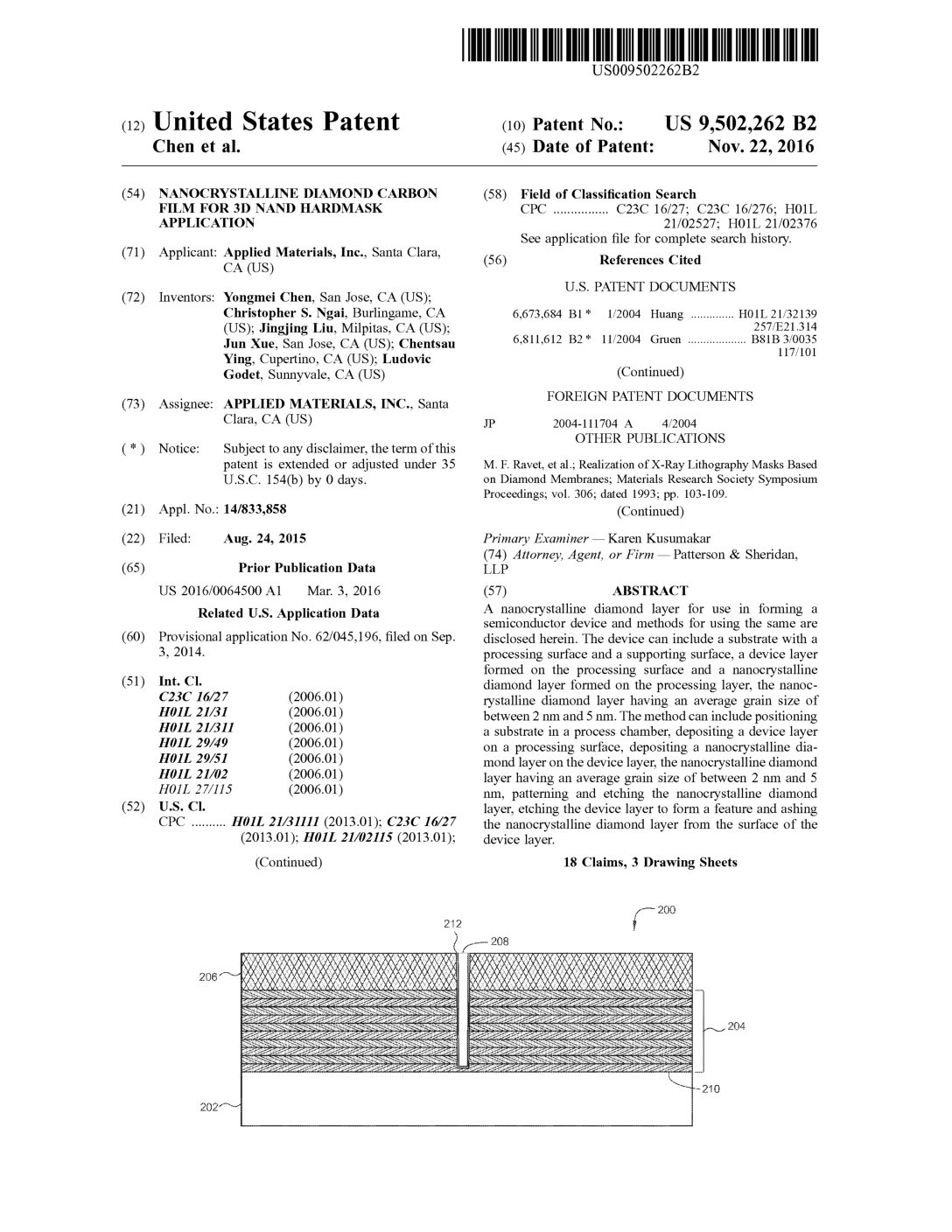
Staff2021-01-31T19:24:49-05:00 US 9,502,262: Nanocrystalline Diamond Carbon Film for 3D NAND Hardmask Application
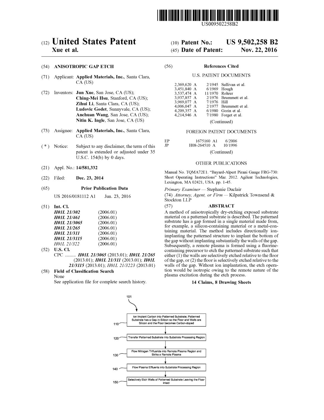
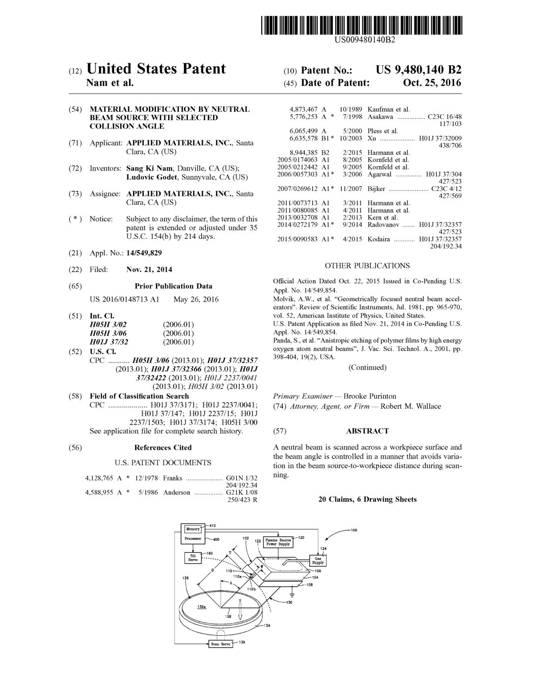
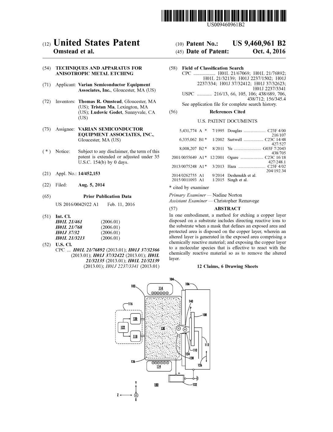
Staff2021-01-31T19:23:37-05:00 US 9,480,140: Material Modification by Neutral Beam Source with Selected Collision Angle
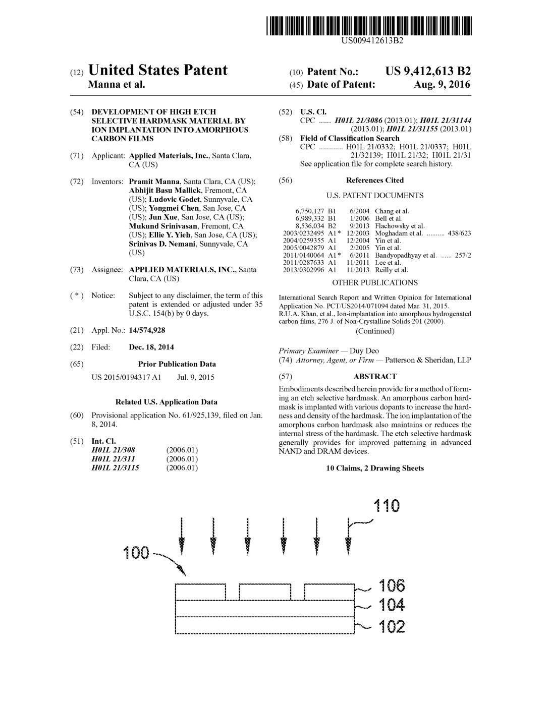
Staff2021-01-31T19:17:36-05:00 US 9,412,613: Development of High Etch Selectivity Hardmask by Ion Implantation in Carbon Films
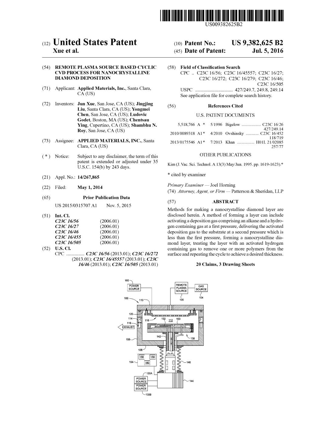
Staff2021-01-31T19:10:44-05:00 US 9,382,625: Remote Plasma Source Based Cyclic CVD Process for Nanocrystalline Diamond Deposition
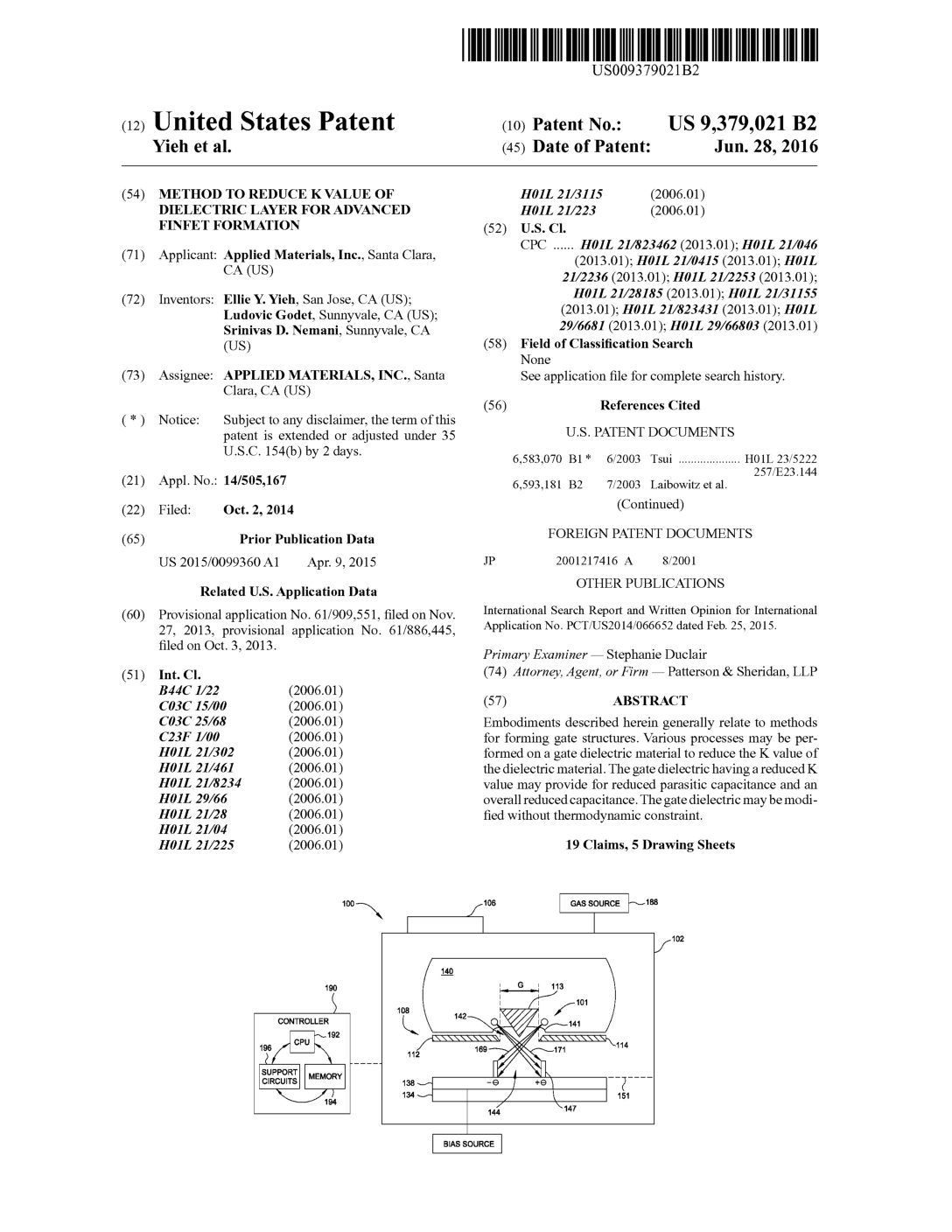
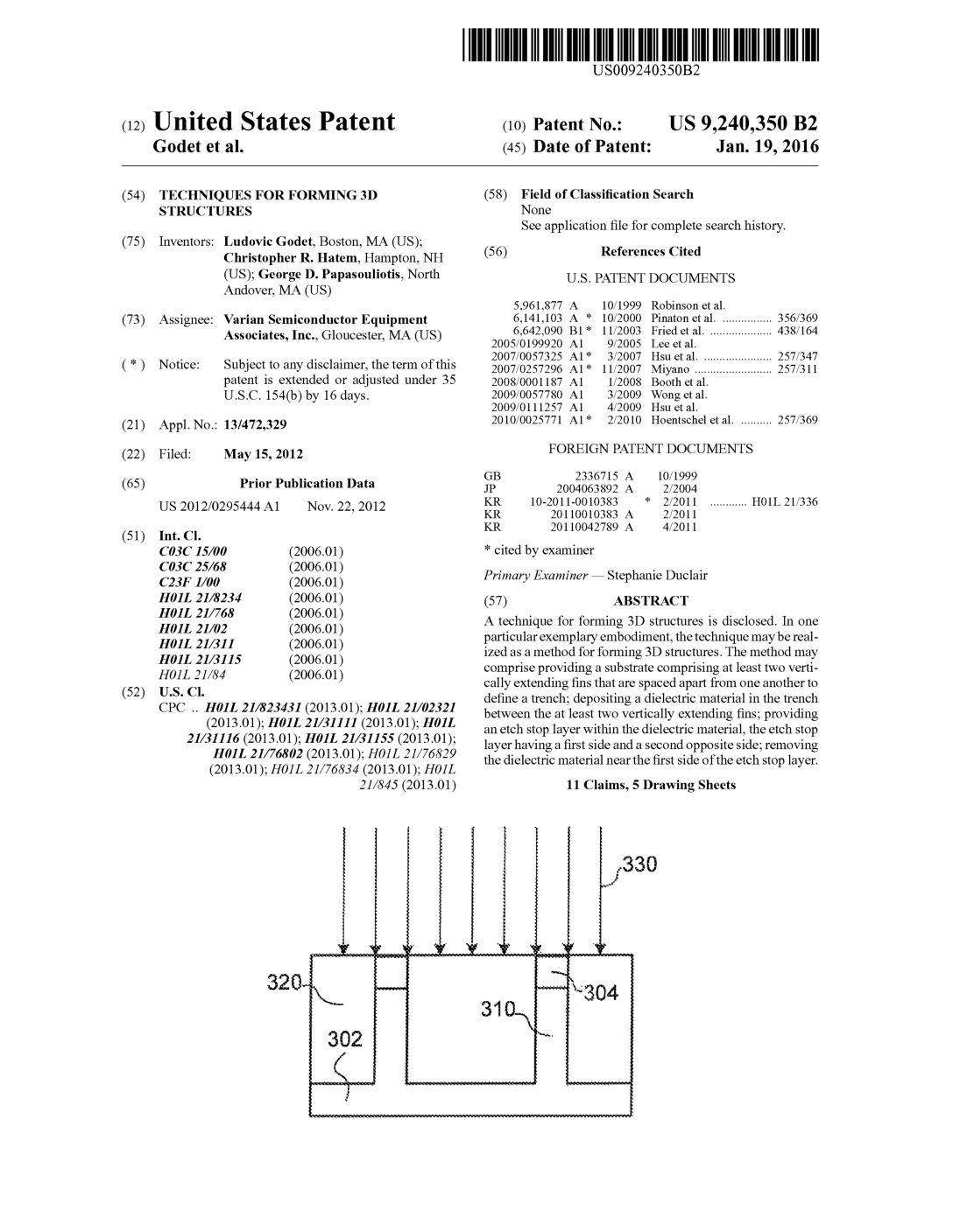
Staff2021-01-31T19:09:08-05:00 US 9,379,021: Method to Reduce K Value of Dielectric Layer for Advanced FinFET Formation
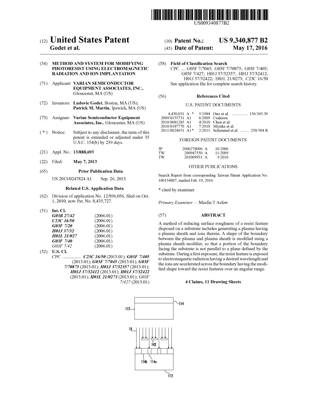
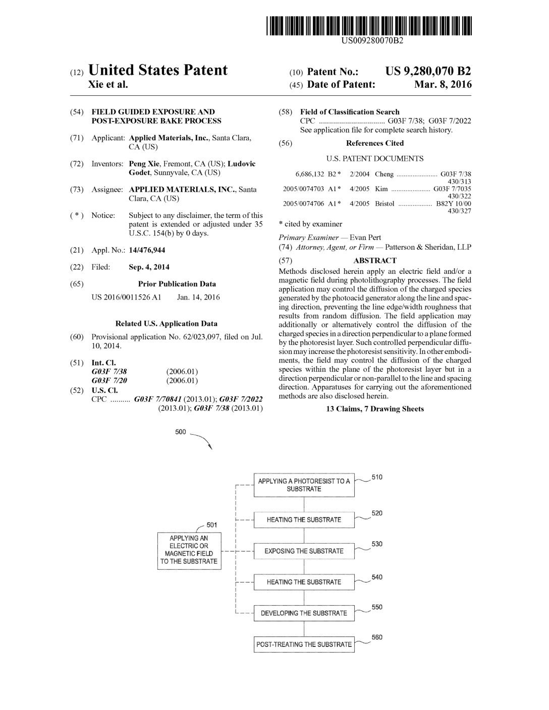
Staff2021-01-31T19:05:56-05:00 US 9,340,877: Method and System for Modifying Photoresist using EM Radiation and Implantation
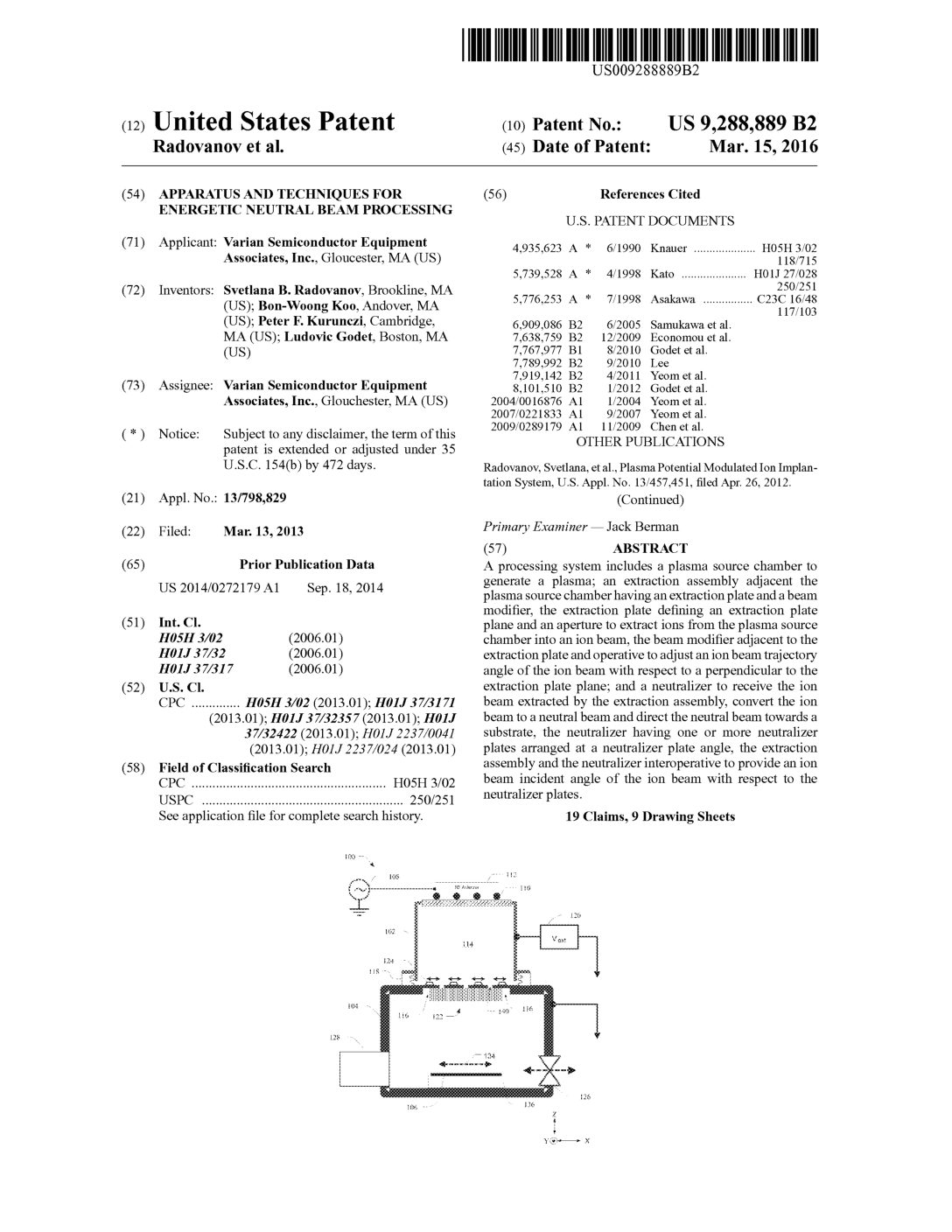
Staff2021-01-31T19:02:05-05:00 US 9,288,889: Apparatus and Techniques for Energetic Neutral Beam Processing
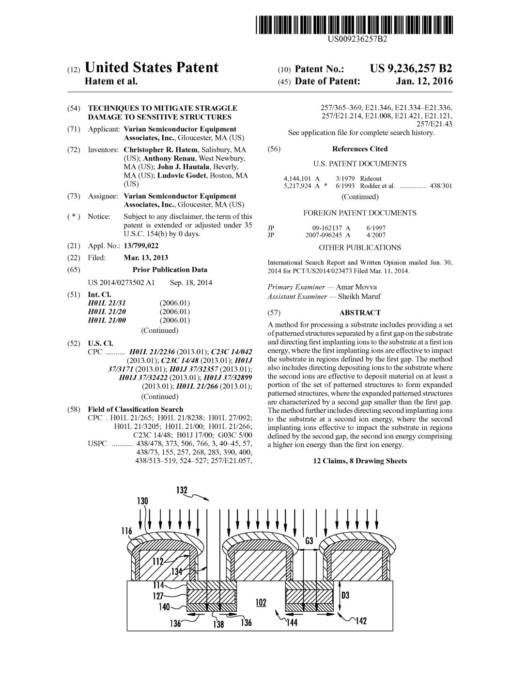
Staff2021-01-31T18:56:21-05:00 US 9,236,257: Techniques to Mitigate Straggle Damage to Sensitive Structures
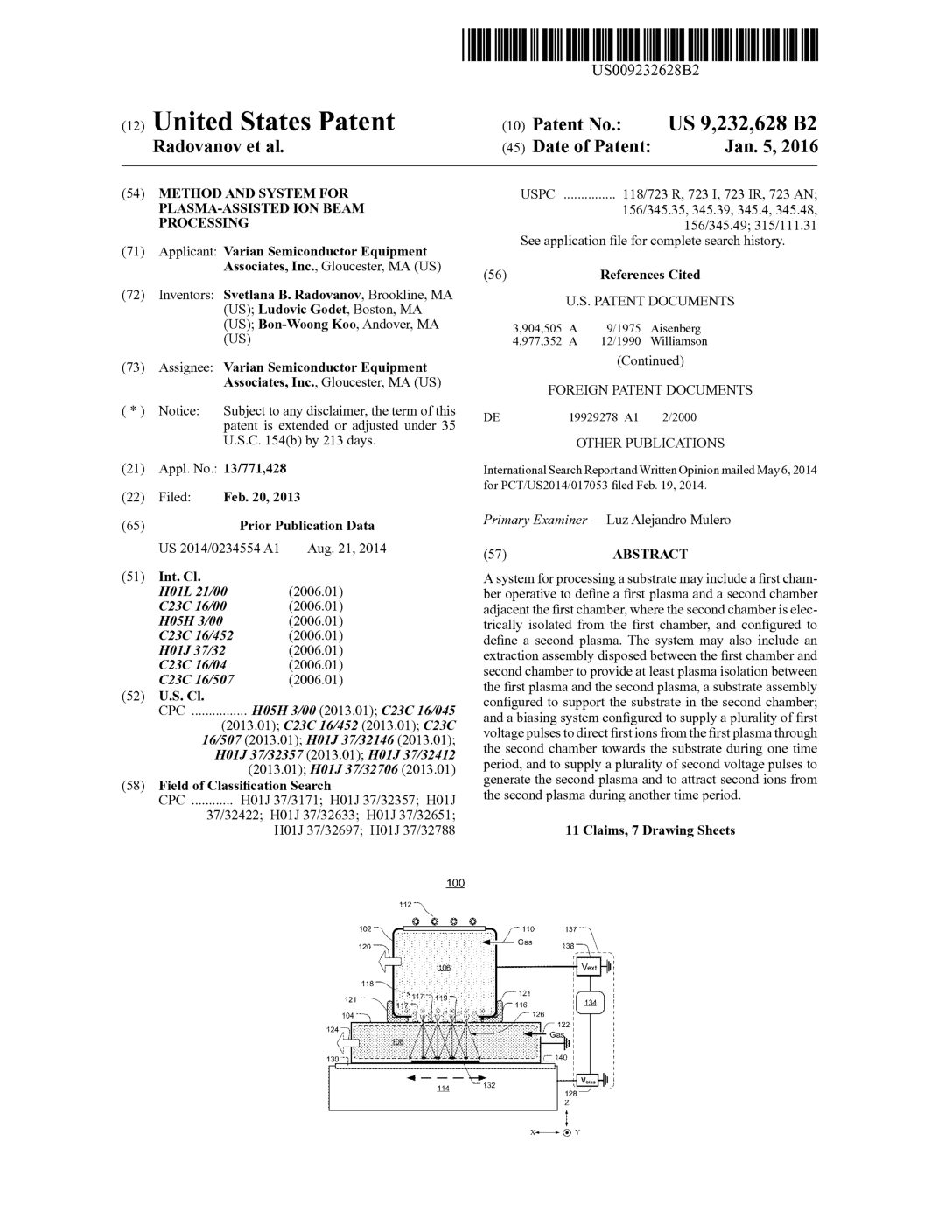
Staff2021-01-31T18:55:14-05:00 US 9,232,628: Method and System for Plasma –Assisted Ion Beam Processing
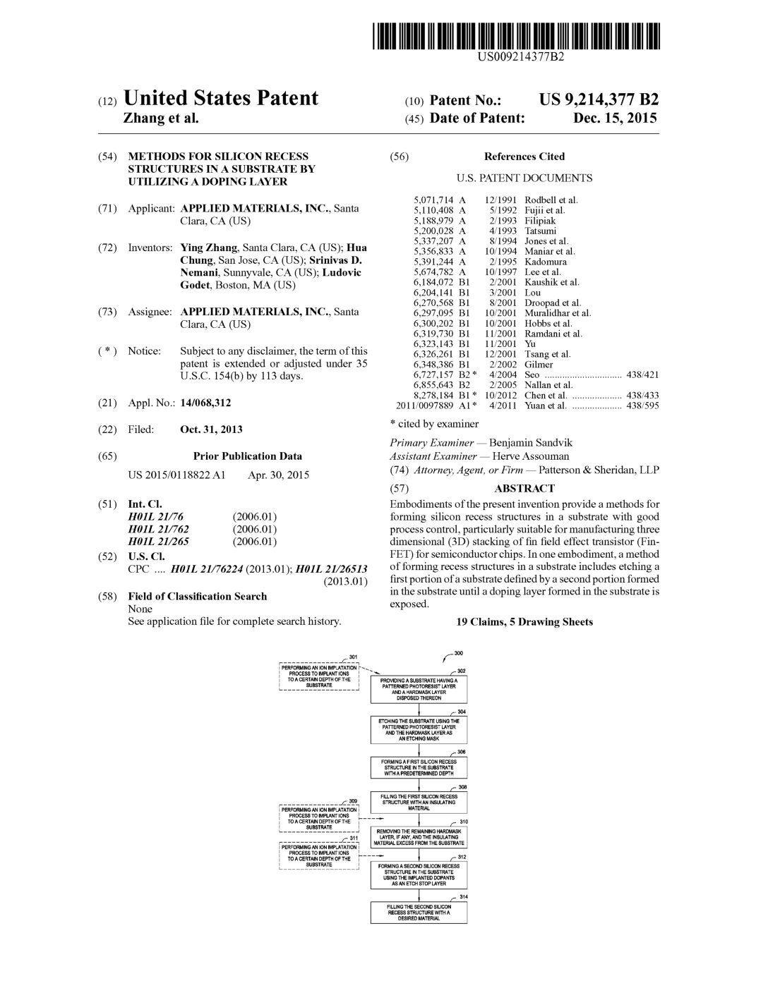
Staff2021-01-31T18:54:16-05:00 US 9,214,377: Methods for Silicon Recess Structure in a Substrate by Utilizing a Doping Layer
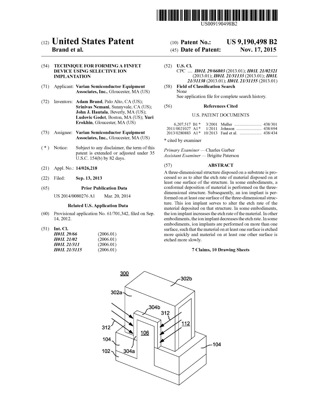
Staff2021-01-31T18:52:41-05:00 US 9,190,498: Technique for Forming a FinFET Device using Selective Ion Implantation
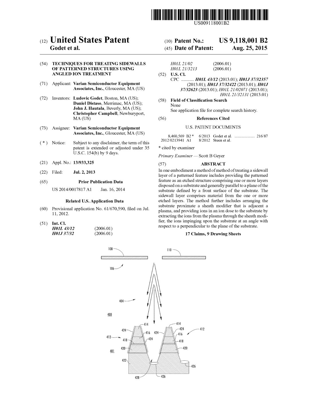
Staff2021-01-31T20:33:44-05:00 US 9,118,001: Techniques for Treating Sidewalls of Patterned Structures using Angled Ion Treatment
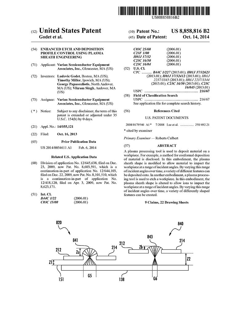
Staff2021-02-04T11:26:34-05:00 US 8,858,816: Enhanced Etch and Deposition Profile Control Using Plasma Sheath Engineering
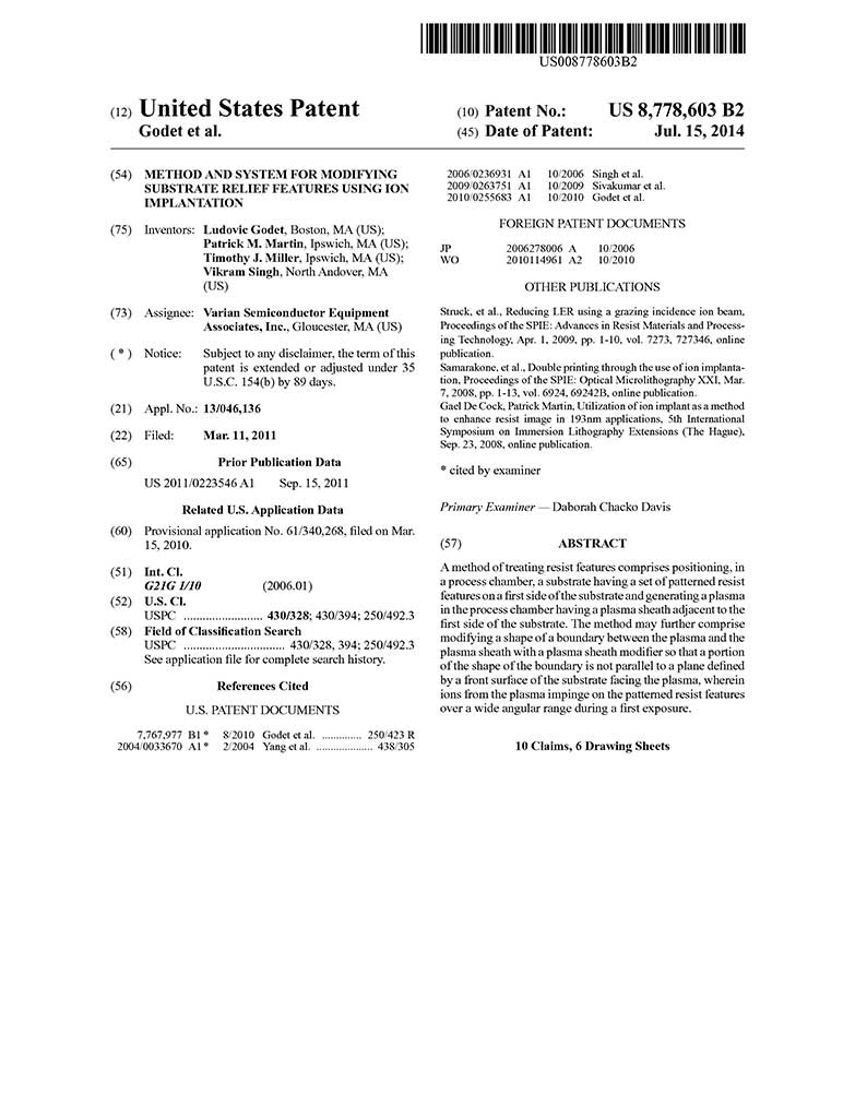
Staff2021-02-04T11:14:27-05:00 US 8,778,603: Method and System for Modifying Substrate Relief Features Using Ion Implantation
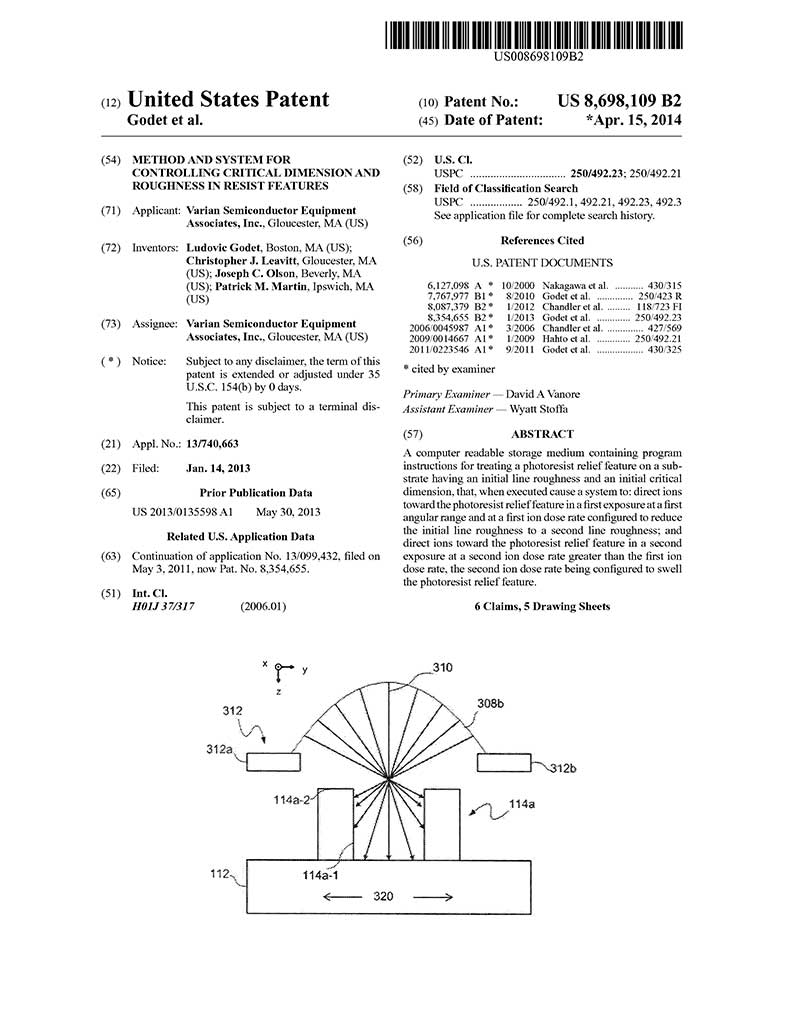
Staff2021-02-04T11:10:37-05:00 US 8,698,109: Method and System for Controlling Critical Dimension and Roughness in Resist Features
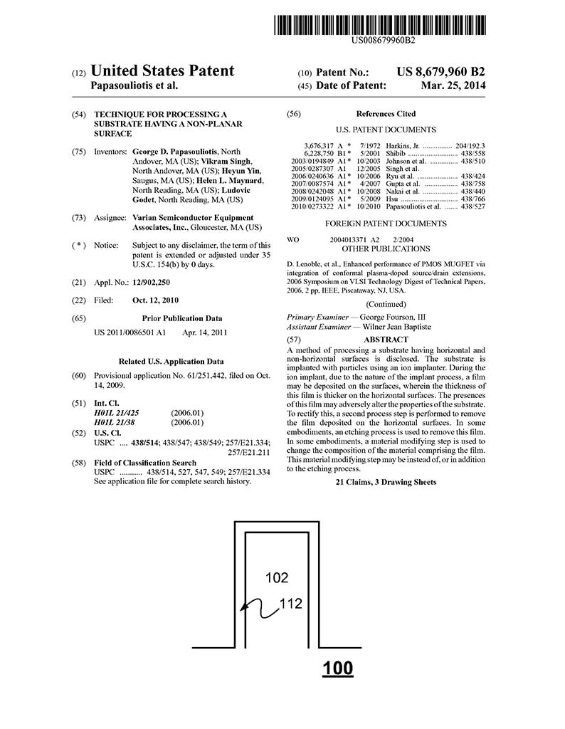
Staff2021-02-04T11:51:09-05:00 US 8,679,960: Technique for Processing a Substrate Having a Non-planar Surface
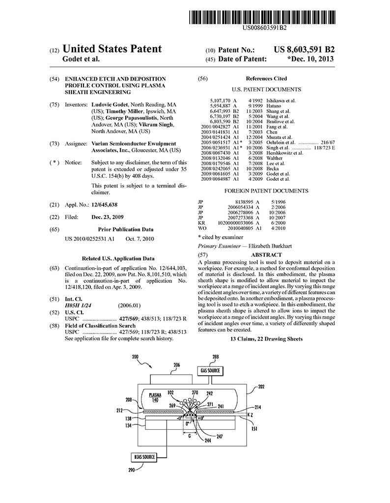
Staff2021-02-04T11:18:33-05:00 US 8,603,591: Enhanced Etch and Deposition Profile Control using Plasma Sheath Engineering
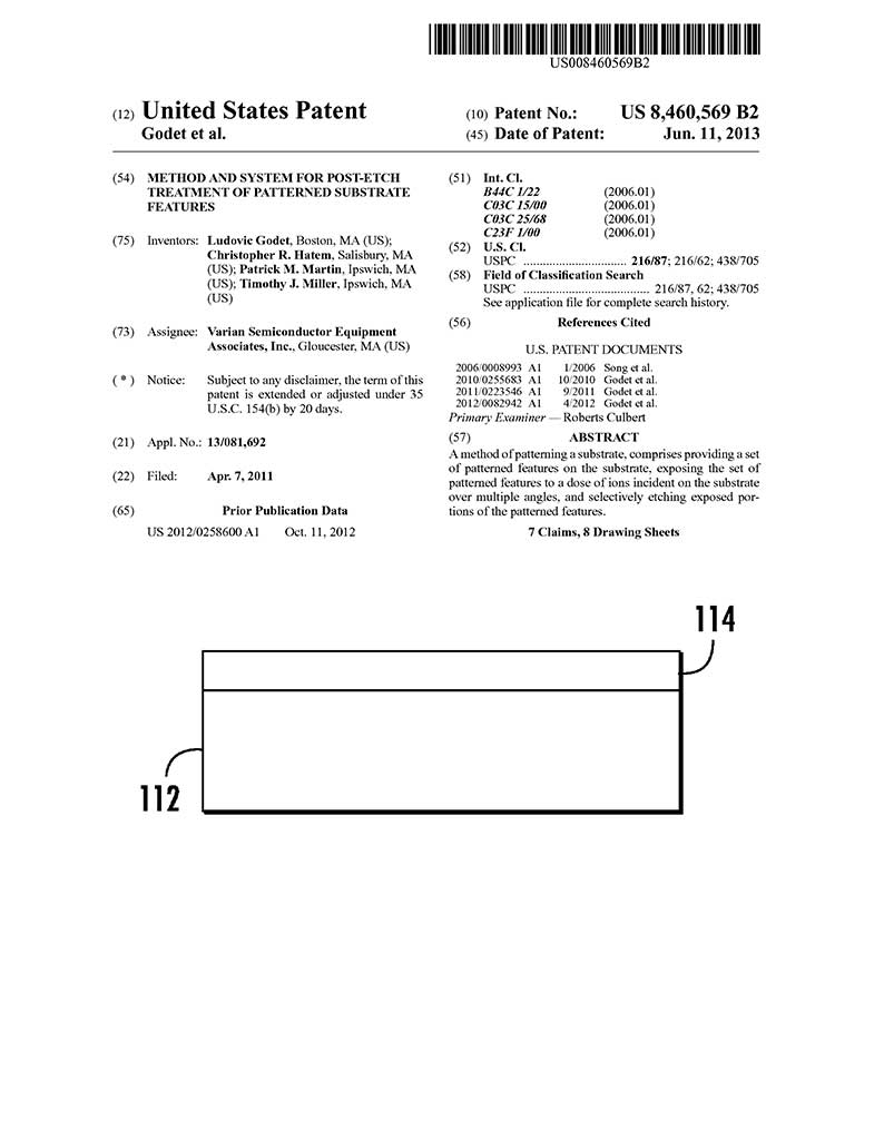
Staff2021-02-04T11:06:17-05:00 US 8,460,569: Method and system for post-etch treatment of patterned substrate features
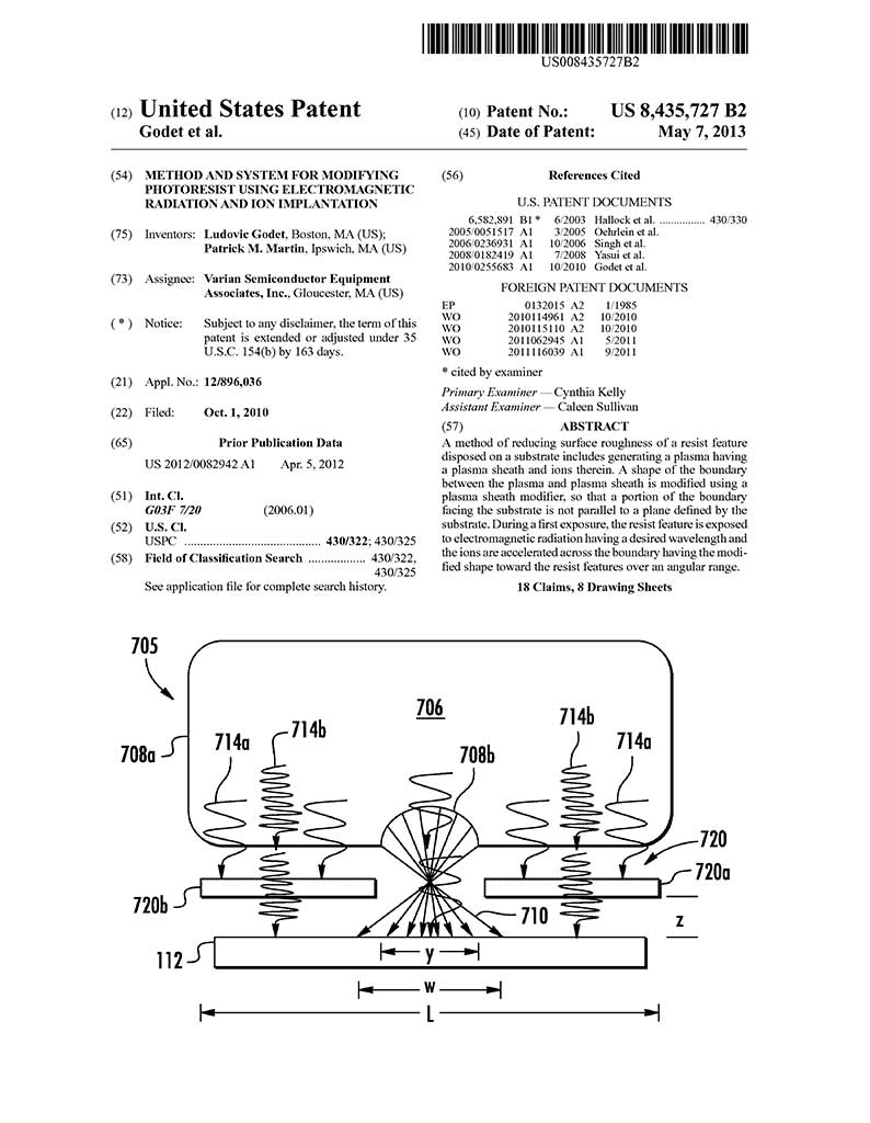
Staff2021-02-03T12:18:41-05:00 US 8,435,727: Method and system for modifying photoresist using electromagnetic radiation and ion implantation
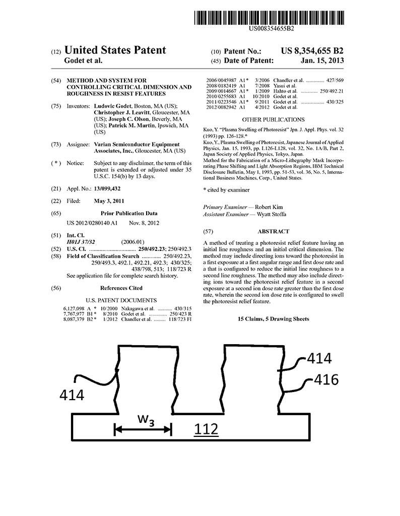
Staff2021-02-03T12:14:09-05:00 US 8,354,655: Method and System for Controlling Critical Dimension and Roughness in Resist Features
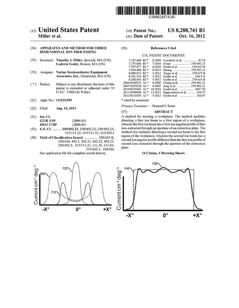
Staff2021-02-05T12:39:42-05:00 US 8,288,741: Apparatus and Method for Three Dimensional Ion Processing
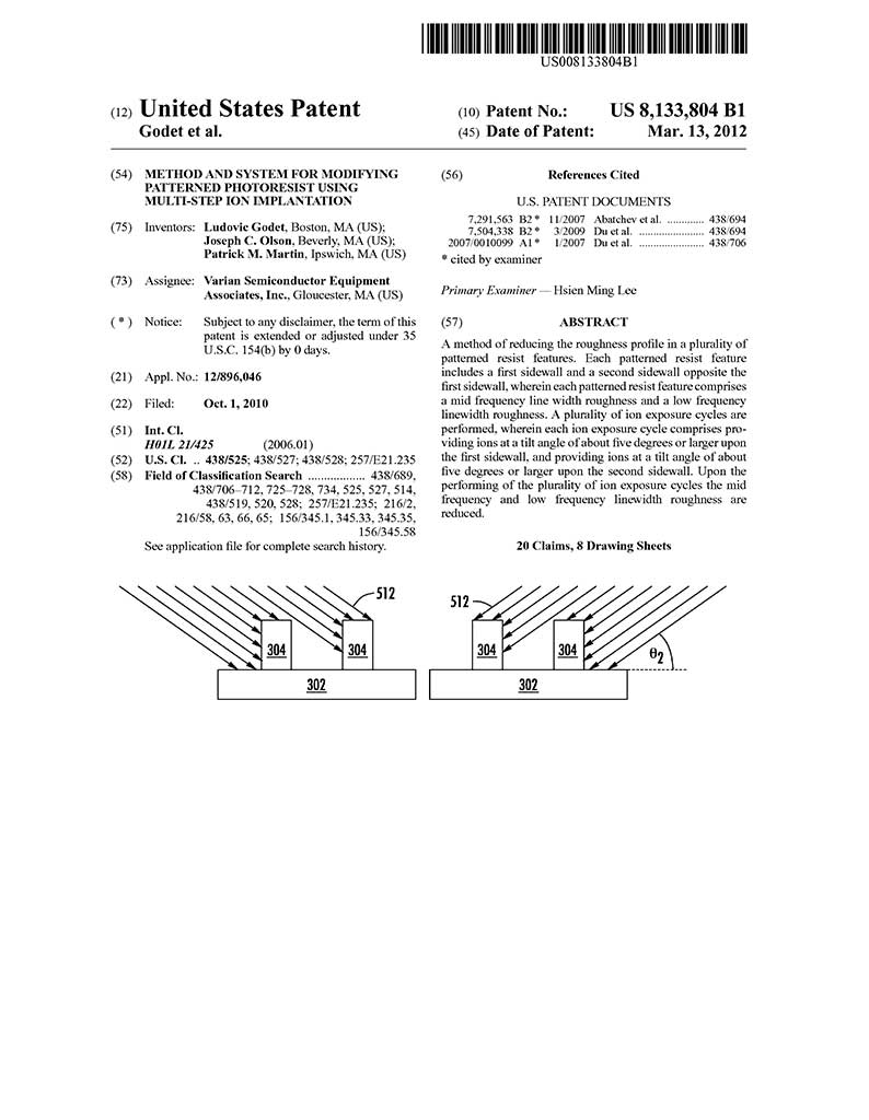
Staff2021-02-03T12:09:26-05:00 US 8,133,804: Method and system for modifying patterned photoresist using multi-step ion implantation
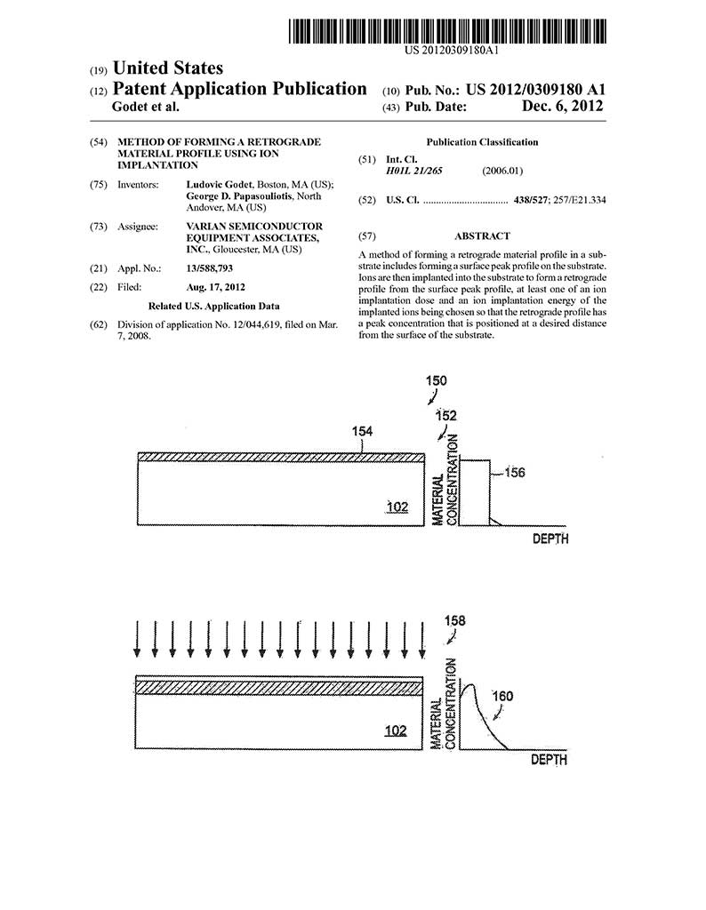
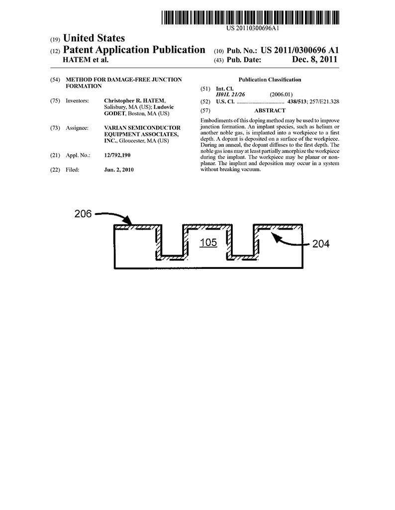
Staff2021-02-02T11:05:56-05:00 US 20120309180: Method of Forming a Retrograde Material Profile Using Ion Implantation
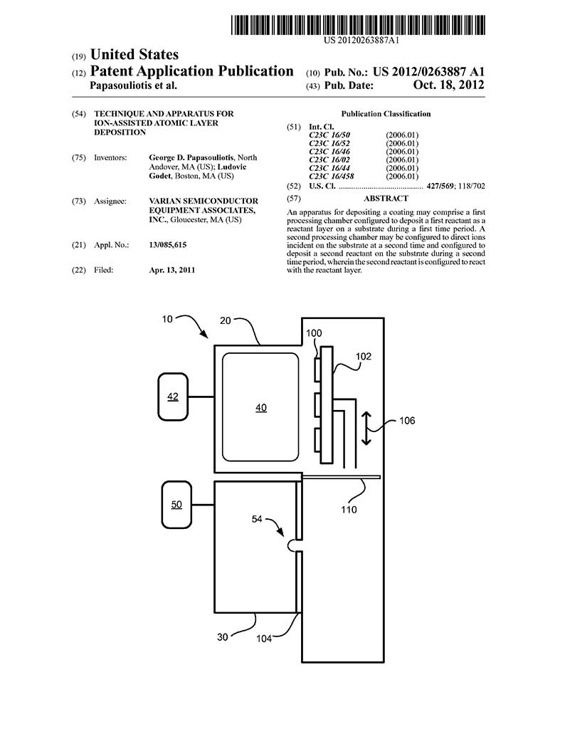
Staff2021-02-02T10:46:28-05:00 US 20120263887: Technique and Apparatus for Ion-Assisted Atomic Layer Deposition
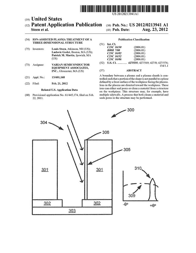
Staff2021-02-02T10:30:19-05:00 US 20120213941: Ion-assisted Plasma Treatment of a Three-dimensional Structure


Social Media