US 9,613,859: Direct Deposition of Nickel Silicide Nanowire
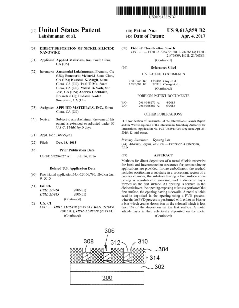
Methods for direct deposition of a metal silicide nanowire for back-end interconnection structures for semiconductor applications are provided. In one embodiment, the method includes positioning a substrate in a processing region of a process chamber, the substrate having a first surface comprising a non-dielectric material; and a dielectric layer formed on the first surface. An opening is formed in the dielectric layer, the opening exposing at least a portion of the first surface, the opening having sidewalls. A metal silicide seed is deposited in the opening using a PVD process, wherein the PVD process is performed with either no bias or a bias which creates deposition on the sidewall which is less than 1% of the deposition on the first surface. A metal silicide layer is then selectively deposited on the metal silicide seed using a metal-silicon organic precursor, creating the metal silicide nanowire.


Social Media