US 10,157,740: Selective deposition process utilizing polymer structure deactivation process
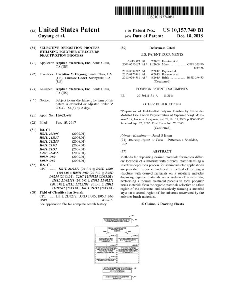
Methods for depositing desired materials formed on different locations of a substrate with different materials using a selective deposition process for semiconductor applications are provided. In one embodiment, a method of forming a structure with desired materials on a substrate includes disposing organic materials on a surface of a substrate, performing a thermal treatment process to form polymer brush materials from the organic materials selective on a first region of the substrate, and selectively forming a material layer on a second region of the substrate uncovered by the polymer brush materials.


Social Media